JAJSGO3C december 2018 – july 2023 LDC5072-Q1
PRODUCTION DATA
- 1
- 1 特長
- 2 アプリケーション
- 3 概要
- 4 Revision History
- 5 概要 (続き)
- 6 Pin Configuration and Functions
- 7 Specifications
- 8 Detailed Description
- 9 Application and Implementation
- 10Power Supply Recommendations
- 11Layout
- 12Device and Documentation Support
- 13Mechanical, Packaging, and Orderable Information
8.3.4 Output Stage
The output stage consists of buffers that drive each of the outputs differentially and maintain the output common mode at VREF_OUT as specified in SpecificationsSpecifications. There are two output stages, one at the OUT0x pins and the other at the OUT1x pins, and each drive the pins in a push-pull manner. For a rotating input, one set of pins will represent the sine angle information and other set will represent cosine angle information. The output stages buffer the AGC output and outputs the final demodulated position information to be used by a microcontroller. The output stage is designed such that it can drive a large range of capacitive loads.
The output stage requires external capacitors as specified by COUT and pullup or pulldown resistors as specified by RPD_OUT and RPU_OUT. The OUTx pins enter a high impedance state in the case of a fault, so the pullup and pulldown resistors are used to pull the voltage out of range for detection by the MCU. See External Diagnostics Required for Loss of VCC or GND for details about external diagnostics required for loss of VCC or GND conditions.
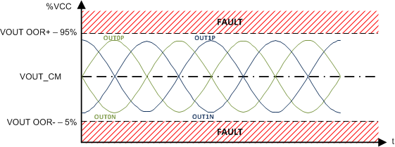
There is a possibility that wires connecting to OUT0 and OUT1 pins can be routed outside the sensor module, so the output stage has both negative and high voltage protection to prevent the part from getting damaged in the event of shorts. The output stage also has out-of-range fault detection. The diagnostic coverage on output stage will also check if the output signal is being driven outside of the maximum allowable limit as defined in SpecificationsSpecifications as shown in Figure 8-4. In the event of a fault, the output stages are put in Hi-Z mode and external pullup and pulldown resistors will drive OUTx pins to maximum and minimum signaling a fault to the microcontroller. See DiagnosticsDiagnosticsDiagnosticsDiagnosticsDiagnosticsDiagnostics for details.
 Figure 8-4 Out of Operation Fault Detection Range at the Output
The voltage at the OUTx pins is not ratiometric to VCC. In AGC mode, the calculated RADIUS in Equation 8 value will change. Only if it crosses one of the threshold (depending on change magnitude of VCC), then the gain of AGC will be adjusted accordingly to bring the RADIUS value back to AGC_TARGET. In fixed-gain mode, the gain will not be adjusted even if VCC change by large magnitude.