SNOSBH0D May 2000 – November 2015 LF156 , LF256 , LF356
PRODUCTION DATA.
- 1 Features
- 2 Applications
- 3 Description
- 4 Revision History
- 5 Pin Configuration and Functions
-
6 Specifications
- 6.1 Absolute Maximum Ratings
- 6.2 ESD Ratings
- 6.3 Recommended Operating Conditions
- 6.4 Thermal Information
- 6.5 AC Electrical Characteristics, TA = TJ = 25°C, VS = ±15 V
- 6.6 DC Electrical Characteristics, TA = TJ = 25°C, VS = ±15 V
- 6.7 DC Electrical Characteristics
- 6.8 Power Dissipation Ratings
- 6.9 Typical Characteristics
- 7 Detailed Description
- 8 Application and Implementation
- 9 Power Supply Recommendations
- 10Layout
- 11Device and Documentation Support
- 12Mechanical, Packaging, and Orderable Information
1 Features
- Advantages
- Replace Expensive Hybrid and Module FET Op Amps
- Rugged JFETs Allow Blow-Out Free Handling Compared With MOSFET Input Devices
- Excellent for Low Noise Applications Using Either High or Low Source Impedance—Very Low 1/f Corner
- Offset Adjust Does Not Degrade Drift or Common-Mode Rejection as in Most Monolithic Amplifiers
- New Output Stage Allows Use of Large Capacitive Loads (5,000 pF) Without Stability Problems
- Internal Compensation and Large Differential Input Voltage Capability
- Common Features
- Low Input Bias Current: 30 pA
- Low Input Offset Current: 3 pA
- High Input Impedance: 1012 Ω
- Low Input Noise Current: 0.01 pA/√Hz
- High Common-Mode Rejection Ratio: 100 dB
- Large DC Voltage Gain: 106 dB
- Uncommon Features
- Extremely Fast Settling Time to 0.01%:
- 4 μs for the LFx55 devices
- 1.5 μs for the LFx56
- 1.5 μs for the LFx57 (AV = 5)
- Fast Slew Rate:
- 5 V/µs for the LFx55
- 12 V/µs for the LFx56
- 50 V/µs for the LFx57 (AV = 5)
- Wide Gain Bandwidth:
- 2.5 MHz for the LFx55 devices
- 5 MHz for the LFx56
- 20 MHz for the LFx57 (AV = 5)
- Low Input Noise Voltage:
- 20 nV/√Hz for the LFx55
- 12 nV/√Hz for the LFx56
- 12 nV/√Hz for the LFx57 (AV = 5)
- Extremely Fast Settling Time to 0.01%:
2 Applications
- Precision High-Speed Integrators
- Fast D/A and A/D Converters
- High Impedance Buffers
- Wideband, Low Noise, Low Drift Amplifiers
- Logarithmic Amplifiers
- Photocell Amplifiers
- Sample and Hold Circuits
3 Description
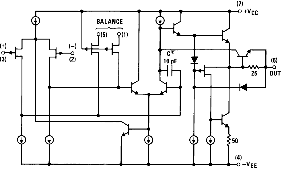
The LFx5x devices are the first monolithic JFET input operational amplifiers to incorporate well-matched, high-voltage JFETs on the same chip with standard bipolar transistors (BI-FET™ Technology). These amplifiers feature low input bias and offset currents/low offset voltage and offset voltage drift, coupled with offset adjust, which does not degrade drift or common-mode rejection. The devices are also designed for high slew rate, wide bandwidth, extremely fast settling time, low voltage and current noise and a low 1/f noise corner.
Device Information(1)
| PART NUMBER | PACKAGE | BODY SIZE (NOM) |
|---|---|---|
| LFx5x | SOIC (8) | 4.90 mm × 3.91 mm |
| TO-CAN (8) | 9.08 mm × 9.08 mm | |
| PDIP (8) | 9.81 mm × 6.35 mm |
- For all available packages, see the orderable addendum at the end of the data sheet.
Simplified Schematic

4 Revision History
Changes from C Revision (March 2013) to D Revision
- Added Pin Configuration and Functions section, ESD Ratings table, Thermal Information table, Feature Description section, Device Functional Modes, Application and Implementation section, Power Supply Recommendations section, Layout section, Device and Documentation Support section, and Mechanical, Packaging, and Orderable Information section Go
- Removed THIGH parameter as it is redundant to TA maximumGo
Changes from B Revision (March 2013) to C Revision
- Changed layout of National Data Sheet to TI formatGo