JAJSE24 October 2017 LM138QML
PRODUCTION DATA.
- 1 特長
- 2 アプリケーション
- 3 概要
- 4 改訂履歴
- 5 Pin Configuration and Functions
- 6 Specifications
- 7 Detailed Description
- 8 Application and Implementation
- 9 Power Supply Recommendations
- 10Layout
- 11デバイスおよびドキュメントのサポート
- 12メカニカル、パッケージ、および注文情報
10 Layout
10.1 Layout Guidelines
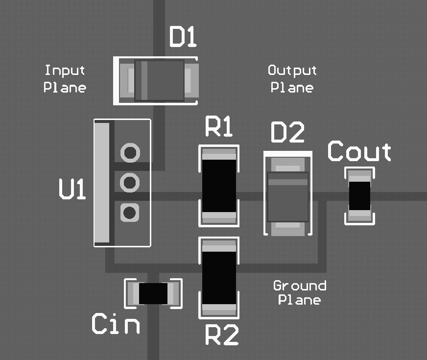
Some layout guidelines must be followed to ensure proper regulation of the output voltage with minimum noise. Traces carrying the load current must be wide to reduce the amount of parasitic trace inductance and the feedback loop from VOUT to ADJ must be kept as short as possible. To improve PSRR, a bypass capacitor can be placed at the ADJ pin and must be placed as close as possible to the device. In cases when VIN shorts to ground, an external diode must be placed from VOUT to VIN to divert the surge current from the output capacitor and protect the deice. Similarly, in cases when a large bypass capacitor is placed at the ADJ pin and VOUT shorts to ground, an external diode must be placed from ADJ to VOUT to provide a path for the bypass capacitor to discharge. These diodes must be placed close to the corresponding device pins to increase their effectiveness.
10.2 Layout Example
 Figure 44. LM138QML Layout