JAJSE24 October 2017 LM138QML
PRODUCTION DATA.
- 1 特長
- 2 アプリケーション
- 3 概要
- 4 改訂履歴
- 5 Pin Configuration and Functions
- 6 Specifications
- 7 Detailed Description
- 8 Application and Implementation
- 9 Power Supply Recommendations
- 10Layout
- 11デバイスおよびドキュメントのサポート
- 12メカニカル、パッケージ、および注文情報
6 Specifications
6.1 Absolute Maximum Ratings
over operating free-air temperature range (unless otherwise noted)(1)| MIN | MAX | UNIT | |
|---|---|---|---|
| Power dissipation | Internally limited | ||
| Input and output voltage differential | –0.3 | 40 | V |
| Storage temperature, Tstg | –65 | 150 | °C |
| Lead temperature (soldering, 10 seconds) | 300 | °C | |
(1) Stresses beyond those listed under Absolute Maximum Ratings may cause permanent damage to the device. These are stress ratings only, which do not imply functional operation of the device at these or any other conditions beyond those indicated under Recommended Operating Conditions. Exposure to absolute-maximum-rated conditions for extended periods may affect device reliability.
6.2 Recommended Operating Conditions
over operating free-air temperature range (unless otherwise noted)| MIN | MAX | UNIT | ||
|---|---|---|---|---|
| Operating temperature, TJ | –55 | 150 | °C | |
| Input-to-output voltage differential | 3 | 40 | V | |
| Output current | 5 | A | ||
6.3 Thermal Information
| THERMAL METRIC(1) | LM138QML | UNIT | |
|---|---|---|---|
| K (TO-3) | |||
| 2 PINS | |||
| RθJA | Junction-to-ambient thermal resistance | 42.8 | °C/W |
| RθJC(top) | Junction-to-case (top) thermal resistance | 3.3 | °C/W |
| ψJT | Junction-to-top characterization parameter | 2.5 | °C/W |
| ψJB | Junction-to-board characterization parameter | 37.4 | °C/W |
(1) For more information about traditional and new thermal metrics, see the IC Package Thermal Metrics application report, SPRA953.
6.4 Electrical Characteristics
Values apply for VIN – VOUT = 5 V; and IOUT = 10 mA (unless otherwise noted)(1)| PARAMETER | TEST CONDITIONS | SUB-GROUPS | MIN | TYP(3) | MAX | UNIT | |
|---|---|---|---|---|---|---|---|
| VREF | Reference voltage | VIN – VOUT = 3 V(5) | [1, 2, 3] | 1.19 | 1.29 | V | |
| VIN – VOUT = 3 V, IOUT = 5 A | [1, 2, 3] | 1.19 | 1.29 | ||||
| VIN – VOUT = 5 V, IOUT = 7 A | [1, 2, 3] | 1.19 | 1.29 | ||||
| VIN – VOUT = 35 V | [1, 2, 3] | 1.19 | 1.29 | ||||
| VIN – VOUT = 35 V, IOUT = 150 mA | [1, 2, 3] | 1.19 | 1.29 | ||||
| VRLINE | Line regulation(2) | 3 V ≤ (VIN – VOUT) ≤ 35 V | [1] | –3.5 | 3.5 | mV | |
| 3.3 V ≤ (VIN – VOUT) ≤ 35 V | [2, 3] | –14 | 14 | ||||
| VRLOAD | Load regulation(2) | VIN – VOUT = 3 V, 10 mA ≤ IOUT ≤ 5 A, VOUT = VREF | [1] | –3.8 | 3.8 | mV | |
| VIN – VOUT = 3.3 V, 10 mA ≤ IOUT ≤ 5 A, VOUT = VREF | [2, 3] | –8 | 8 | ||||
| VIN – VOUT = 35 V, 10 mA ≤ IOUT ≤ 150 mA, VOUT = VREF | [1] | –3.8 | 3.8 | ||||
| [2, 3] | –8 | 8 | |||||
| VRTH | Thermal regulation | VIN – VOUT = 10 V, pulse = 20 ms, IOUT = 1 A(4) |
[1] | 0.002 | 0.01 | %/W | |
| IADJ | Adjustment pin current | VIN – VOUT = 3 V(5) | [1, 2, 3] | 2 | 45 | 100 | μA |
| VIN – VOUT = 35 V | [1, 2, 3] | 2 | 100 | ||||
| ΔIADJ | Adjustment pin current change | 3 V ≤ (VIN – VOUT) ≤ 35 V(5) | [1, 2, 3] | –5 | 0.2 | 5 | μA |
| 10 mA ≤ IOUT ≤ 5 A | [1, 2, 3] | –5 | 5 | ||||
| ILOAD(MIN) | Minimum load current | VIN – VOUT = 3 V, VOUT = 1.4 V(5) | [1, 2, 3] | 0.5 | 5 | mA | |
| VIN – VOUT = 35 V, VOUT = 1.4 V | [1, 2, 3] | 0.5 | 3.5 | 5 | |||
| ICL | Current limit | VIN – VOUT = 10 V, T = 0.5 ms, VOUT = 0 V |
[1, 2, 3] | 7 | 16 | A | |
| T = 5 ms, VOUT = 0 V | [1, 2, 3] | 5 | 15 | ||||
| ΔVR/ΔVIN | Ripple rejection ratio | VOUT = VREF, eIN = 1 VRMS, f = 120 Hz, IOUT = 500 mA(6) | [4] | 60 | dB | ||
(1) These specifications are applicable for power dissipations up to 50W. Power dissipation is specified at these values up to 15-V input-output differential. Above 15-V differential, power dissipation will be limited by internal protection circuitry. All limits (that is, the numbers in the minimum and maximum columns) are specified to TI's AOQL (Average Outgoing Quality Level).
(2) Regulation is measured at a constant junction temperature, using pulse testing with a low duty cycle. Changes in output voltage due to heating effects are covered under the specifications for thermal regulation.
(3) Typical figures are at TA = 25°C, and represent most likely parametric norms. Test limits are ensured to Texas Instruments' average outgoing quality level (AOQL).
(4) Datalog reading in mV, 0.01% = 1.19 mV.
(5) VIN – VOUT = 3.3 V at –55°C and 125°C.
(6) Family board not required for this device.
6.5 Quality Conformance Inspection
MIL-STD-883, Method 5005 - Group A
| SUBGROUP | DESCRIPTION | TEMPERATURE (°C) |
|---|---|---|
| 1 | Static tests at | 25 |
| 2 | Static tests at | 125 |
| 3 | Static tests at | –55 |
| 4 | Dynamic tests at | 25 |
| 5 | Dynamic tests at | 125 |
| 6 | Dynamic tests at | –55 |
| 7 | Functional tests at | 25 |
| 8A | Functional tests at | 125 |
| 8B | Functional tests at | –55 |
| 9 | Switching tests at | 25 |
| 10 | Switching tests at | 125 |
| 11 | Switching tests at | –55 |
| 12 | Setting time at | 25 |
| 13 | Setting time at | 125 |
| 14 | Setting time at | –55 |
6.6 Typical Performance Characteristics
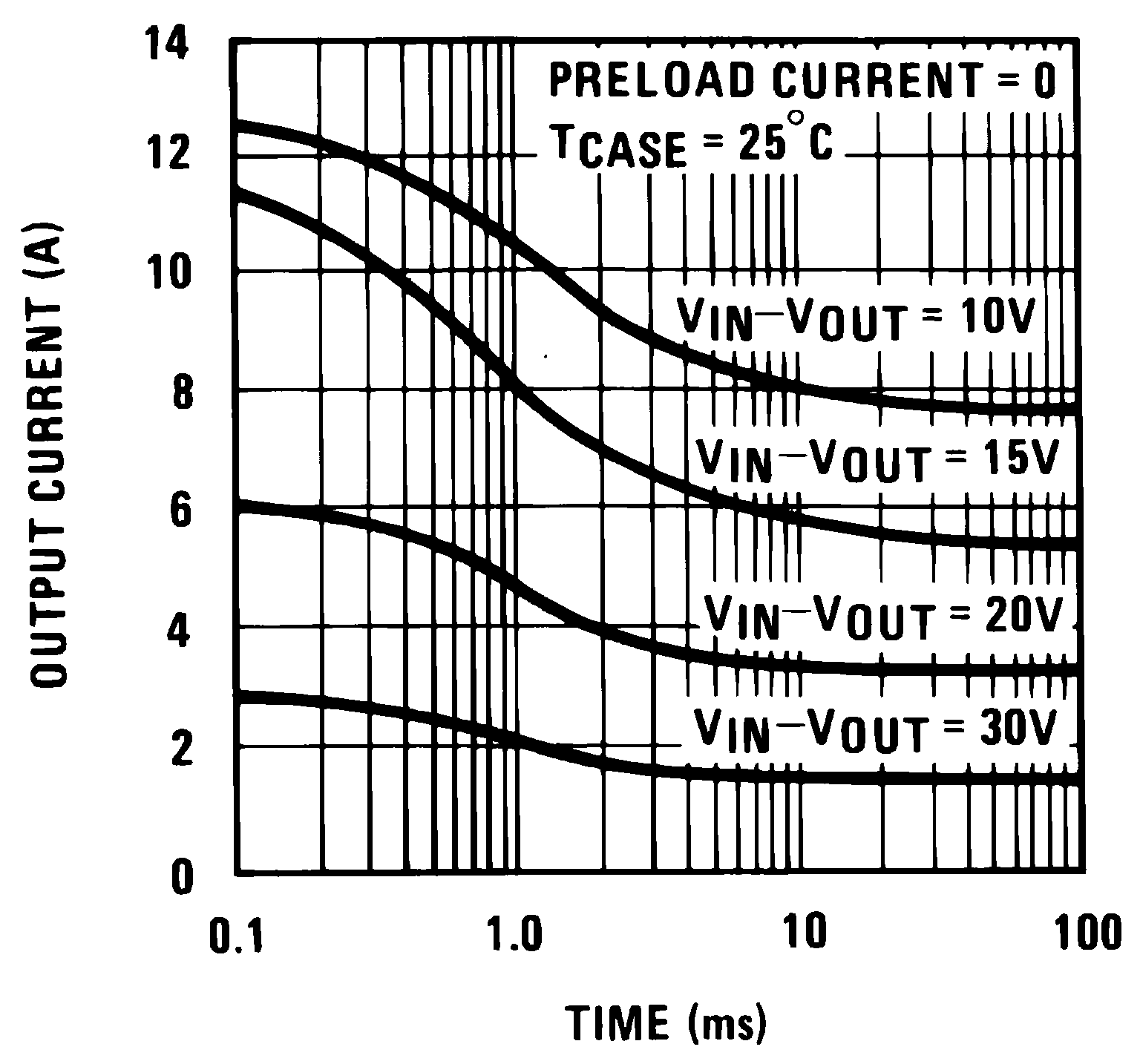 Figure 1. Current Limit
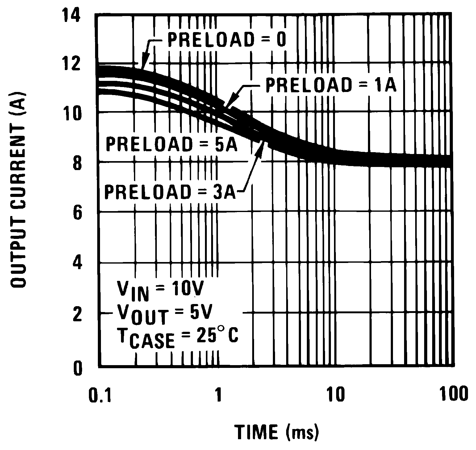 Figure 3. Current Limit
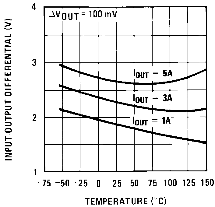 Figure 5. Dropout Voltage
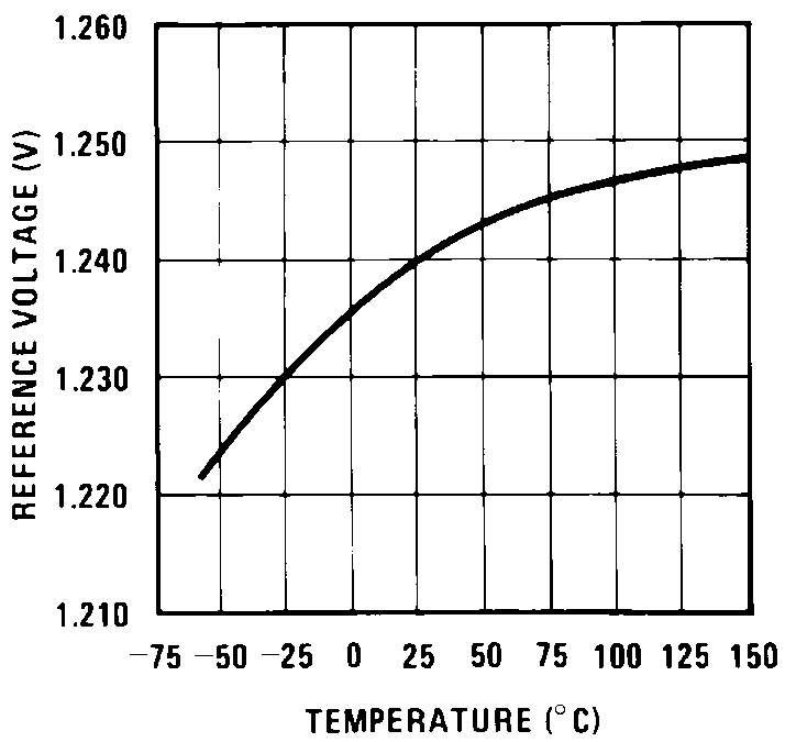 Figure 7. Temperature Stability
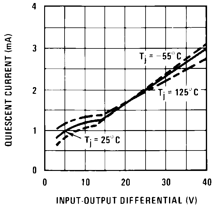 Figure 9. Minimum Operating Current
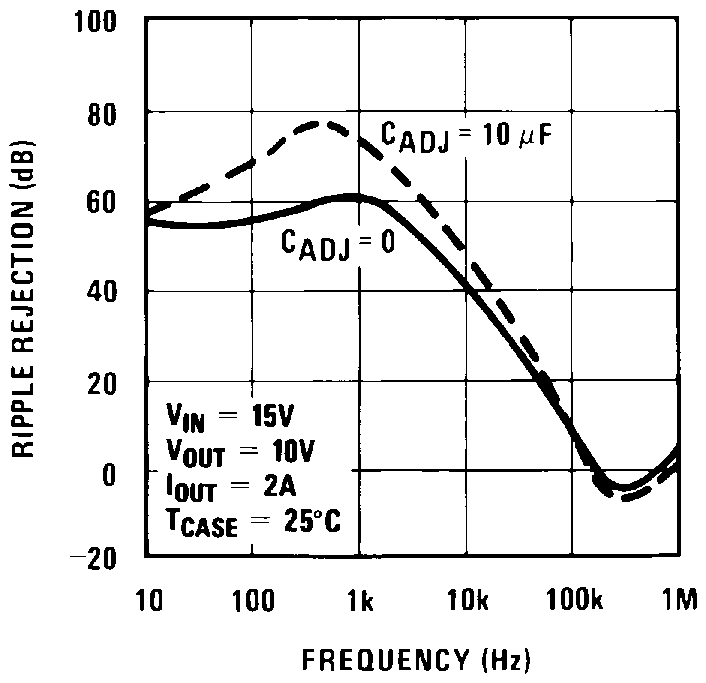 Figure 11. Ripple Rejection
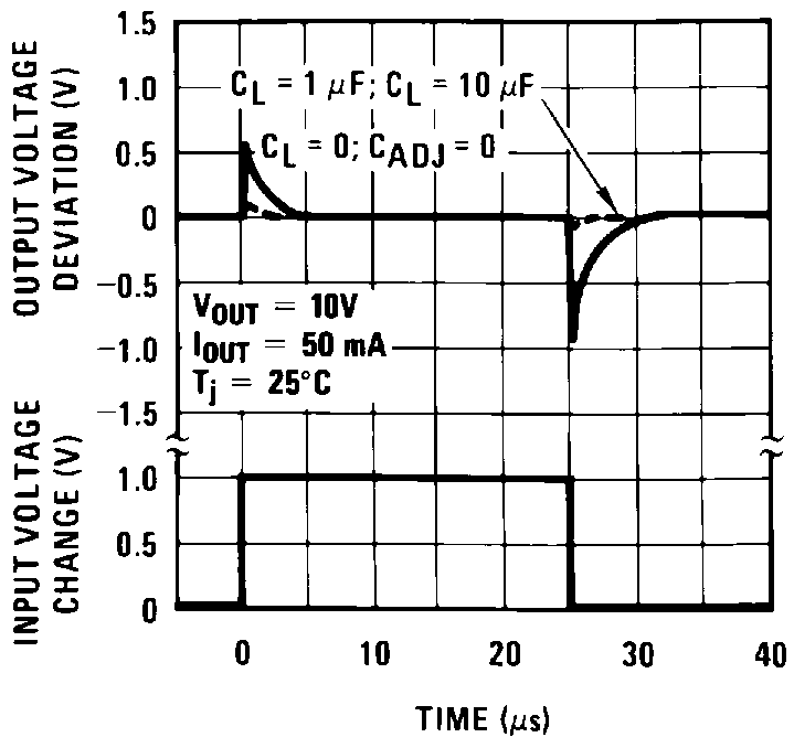 Figure 13. Line Transient Response
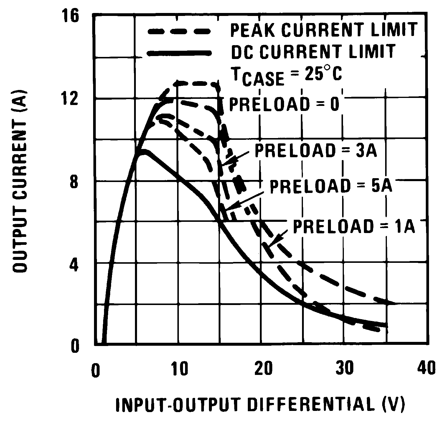 Figure 2. Current Limit
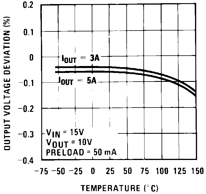 Figure 4. Load Regulation
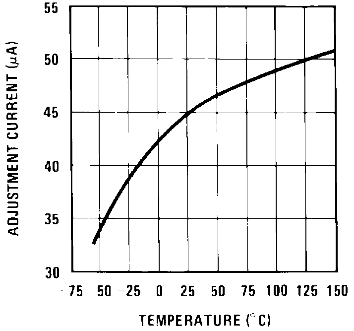 Figure 6. Adjustment Current
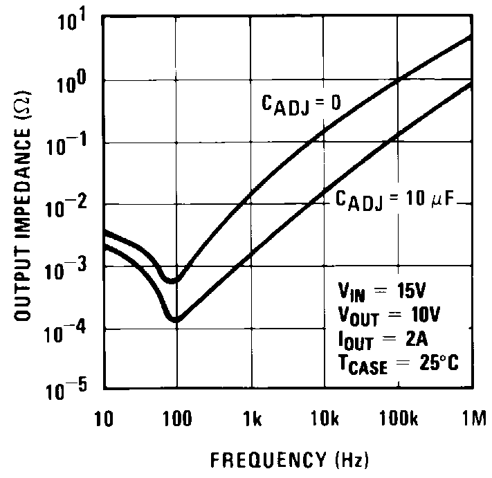 Figure 8. Output Impedance
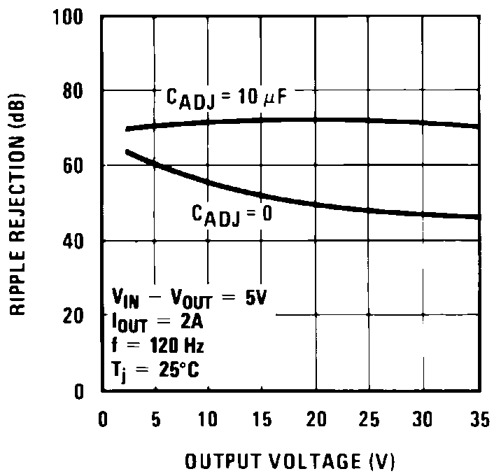 Figure 10. Ripple Rejection
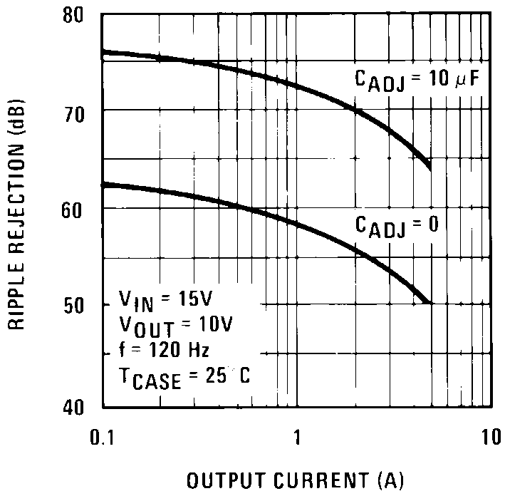 Figure 12. Ripple Rejection
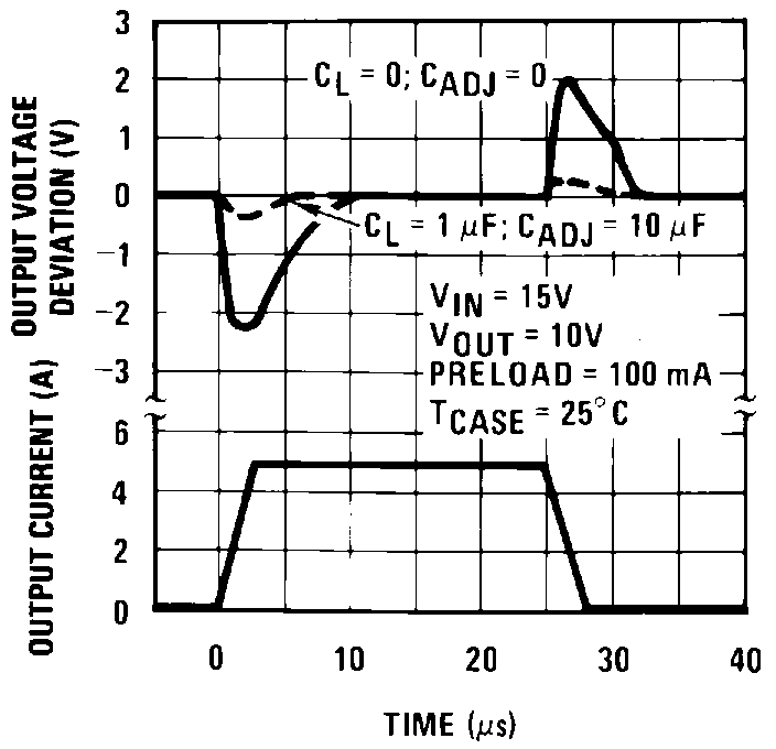 Figure 14. Load Transient Response