JAJSDB8 June 2017 LM139-MIL
- 1 特長
- 2 アプリケーション
- 3 概要
- 4 改訂履歴
- 5 Pin Configuration and Functions
- 6 Specifications
- 7 Detailed Description
- 8 Application and Implementation
- 9 Power Supply Recommendations
- 10Layout
- 11デバイスおよびドキュメントのサポート
- 12メカニカル、パッケージ、および注文情報
パッケージ・オプション
メカニカル・データ(パッケージ|ピン)
サーマルパッド・メカニカル・データ
発注情報
6 Specifications
6.1 Absolute Maximum Ratings
over operating free-air temperature range (unless otherwise noted)(1)| MIN | MAX | UNIT | |||
|---|---|---|---|---|---|
| VCC | Supply voltage(2) | 36 | V | ||
| VID | Differential input voltage(3) | ±36 | V | ||
| VI | Input voltage range (either input) | –0.3 | 36 | V | |
| IK | Input current(5) | –50 | mA | ||
| VO | Output voltage | 36 | V | ||
| IO | Output current | 20 | mA | ||
| Duration of output short circuit to ground(4) | Unlimited | ||||
| TJ | Operating virtual-junction temperature | 150 | °C | ||
| Case temperature for 60 s | FK package | 260 | °C | ||
| Lead temperature 1.6 mm (1/16 in) from case for 60 s | J package | 300 | °C | ||
| Tstg | Storage temperature | –65 | 150 | °C | |
(1) Stresses beyond those listed under Absolute Maximum Ratings may cause permanent damage to the device. These are stress ratings only, and functional operation of the device at these or any other conditions beyond those indicated under Recommended Operating Conditions is not implied. Exposure to absolute-maximum-rated conditions for extended periods may affect device reliability.
(2) All voltage values, except differential voltages, are with respect to network ground.
(3) Differential voltages are at xIN+ with respect to xIN–.
(4) Short circuits from outputs to VCC can cause excessive heating and eventual destruction.
(5) Input current flows through parasitic diode to ground and will turn on parasitic transistors that will increase ICC and may cause output to be incorrect. Normal operation resumes when input is removed.
6.2 ESD Ratings
| VALUE | UNIT | |||
|---|---|---|---|---|
| V(ESD) | Electrostatic discharge | Human body model (HBM), per ANSI/ESDA/JEDEC JS-001(1) | ±500 | V |
| Charged-device model (CDM), per JEDEC specification JESD22-C101(2) | ±750 | |||
(1) JEDEC document JEP155 states that 500-V HBM allows safe manufacturing with a standard ESD control process.
(2) JEDEC document JEP157 states that 250-V CDM allows safe manufacturing with a standard ESD control process.
6.3 Recommended Operating Conditions
over operating free-air temperature range (unless otherwise noted)| MIN | MAX | UNIT | |||
|---|---|---|---|---|---|
| VCC | Supply voltage | 2 | 30 | V | |
| TJ | Junction temperature | –55 | 125 | °C | |
6.4 Thermal Information
| THERMAL METRIC(1) | LM139-MIL | UNIT | ||||
|---|---|---|---|---|---|---|
| D (SOIC) | J (CDIP) | W (CFP) | FK (LCCC) | |||
| RθJA | Junction-to-ambient thermal resistance | 98.8 | 89.5 | 156.2 | 82.5 | °C/W |
| RθJC(top) | Junction-to-case (top) thermal resistance | 64.3 | 46.1 | 86.7 | 60.7 | °C/W |
| RθJB | Junction-to-board thermal resistance | 59.7 | 78.7 | 154.6 | 59.4 | °C/W |
| ψJT | Junction-to-top characterization parameter | 25.7 | 3 | 56.5 | 53 | °C/W |
| ψJB | Junction-to-board characterization parameter | 59.3 | 71.8 | 133.5 | 58.4 | °C/W |
| RθJC(bot) | Junction-to-case (bottom) thermal resistance | — | 24.2 | 14.3 | 9.7 | °C/W |
(1) For more information about traditional and new thermal metrics, see the Semiconductor and IC Package Thermal Metrics application report.
6.5 Electrical Characteristics
at specified free-air temperature, VCC = 5 V (unless otherwise noted)| PARAMETER | TEST CONDITIONS(1) | MIN | TYP | MAX | UNIT | |||
|---|---|---|---|---|---|---|---|---|
| VIO | Input offset voltage | VCC = 5 V to 30 V, VIC = VICR min, VO = 1.4 V |
TA = 25°C | 2 | 5 | mV | ||
| TA = –55°C to +125°C | 9 | |||||||
| IIO | Input offset current | VO = 1.4 V | TA = 25°C | 3 | 25 | nA | ||
| TA = –55°C to +125°C | 100 | |||||||
| IIB | Input bias current | VO = 1.4 V | TA = 25°C | –25 | –100 | nA | ||
| TA = –55°C to +125°C | –300 | |||||||
| VICR | Common-mode input-voltage range(2) | TA = 25°C | 0 to VCC – 1.5 |
V | ||||
| TA = –55°C to +125°C | 0 to VCC – 2 |
|||||||
| AVD | Large-signal differential-voltage amplification | VCC+ = ±7.5 V, VO = –5 V to +5 V |
TA = 25°C | 200 | V/mV | |||
| IOH | High-level output current | VID = 1 V | VOH = 5 V | TA = 25°C | 0.1 | nA | ||
| VOH = 30 V | TA = –55°C to +125°C | 1 | μA | |||||
| VOL | Low-level output voltage | VID = –1 V, | IOL = 4 mA | TA = 25°C | 150 | 400 | mV | |
| TA = –55°C to +125°C | 700 | |||||||
| IOL | Low-level output current | VID = –1 V, | VOL = 1.5 V | TA = 25°C | 6 | 16 | mA | |
| ICC | Supply current (four comparators) |
VO = 2.5 V, | No load | TA = 25°C | 0.8 | 2 | mA | |
(1) All characteristics are measured with zero common-mode input voltage, unless otherwise specified.
(2) The voltage at either input or common-mode must not be allowed to go negative by more than 0.3 V. The upper end of the common-mode voltage range is VCC+ – 1.5 V; however, one input can exceed VCC, and the comparator will provide a proper output state as long as the other input remains in the common-mode range. Either or both inputs can go to 30 V without damage.
6.6 Switching Characteristics
VCC = 5 V, TA = 25°C| PARAMETER | TEST CONDITIONS | TYP | UNIT | |
|---|---|---|---|---|
| Response time | RL connected to 5 V through 5.1 kΩ, CL = 15 pF(1)(2) |
100-mV input step with 5-mV overdrive | 1.3 | μs |
| TTL-level input step | 0.3 | |||
(1) CL includes probe and jig capacitance.
(2) The response time specified is the interval between the input step function and the instant when the output crosses 1.4 V.
6.7 Typical Characteristics
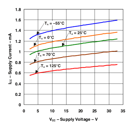 Figure 1. Supply Current vs Supply Voltage
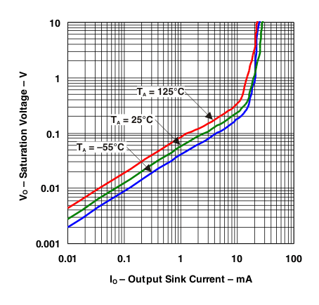 Figure 3. Output Saturation Voltage
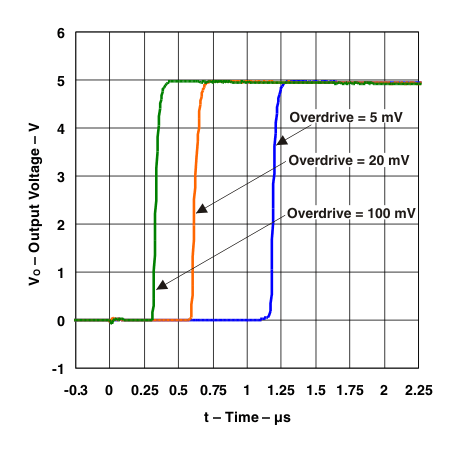 Figure 5. Response Time for Various Overdrives
 Positive Transition
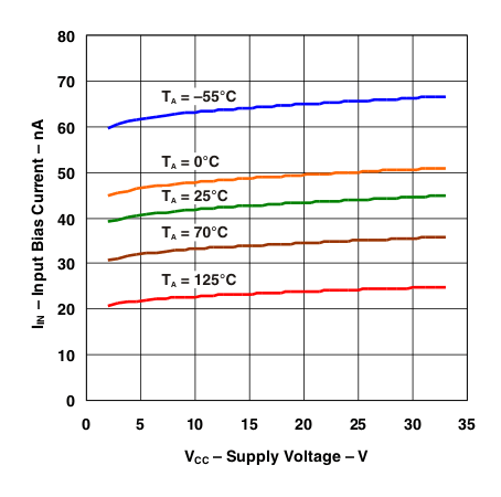 Figure 2. Input Bias Current vs Supply Voltage
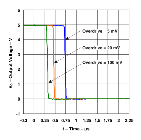 Figure 4. Response Time for Various Overdrives
Negative Transition