SNVS528H October 2007 – January 2016 LM20143 , LM20143-Q1
PRODUCTION DATA.
- 1 Features
- 2 Applications
- 3 Description
- 4 Revision History
- 5 Pin Configuration and Functions
- 6 Specifications
- 7 Detailed Description
-
8 Application and Implementation
- 8.1 Application Information
- 8.2
Typical Applications
- 8.2.1
3.3-V or 5-V Supply Rail Design
- 8.2.1.1 Design Requirements
- 8.2.1.2
Detailed Design Procedure
- 8.2.1.2.1 Duty Cycle Calculation
- 8.2.1.2.2 Inductor Selection (L)
- 8.2.1.2.3 Output Capacitor Selection (COUT)
- 8.2.1.2.4 Input Capacitor Selection (CIN)
- 8.2.1.2.5 Setting the Output Voltage (RFB1, RFB2)
- 8.2.1.2.6 Adjusting the Operating Frequency (RT)
- 8.2.1.2.7 AVIN Filtering Components (CF and RF)
- 8.2.1.2.8 Sub-Regulator Bypass Capacitor (CVCC)
- 8.2.1.2.9 Setting the Start Up Time (CSS)
- 8.2.1.2.10 Loop Compensation (RC1, CC1)
- 8.2.1.3 Application Curves
- 8.2.2 5-V Supply Rail Design
- 8.2.3 3-V Supply Rail Design
- 8.2.1
3.3-V or 5-V Supply Rail Design
- 9 Power Supply Recommendations
- 10Layout
- 11Device and Documentation Support
- 12Mechanical, Packaging, and Orderable Information
8 Application and Implementation
NOTE
Information in the following applications sections is not part of the TI component specification, and TI does not warrant its accuracy or completeness. TI’s customers are responsible for determining suitability of components for their purposes. Customers should validate and test their design implementation to confirm system functionality.
8.1 Application Information
The LM20143 is a step down DC/DC converter, typically used for to convert 3.3 V or 5 V rail to lower DC voltages with a maximum output current of 3 A. The following design procedure can be used to select all the external components for the LM20143. Alternately, the WEBENCH® Design Tool may be used to complete the design. By using this tool the user can optimize the design by using an iterative design procedure and selecting different components from the extensive component database. Along with this datasheet and WEBENCH, the user can reference the LM20143 Quickstart Calculator tool as a free download. The Quickstart tool is an excel sheet summary of the Typical Applications section.
8.2 Typical Applications
Several circuit designs can be created for applications with differing requirements. Three examples demonstrating this are detailed in this section.
8.2.1 3.3-V or 5-V Supply Rail Design
This section walks the designer through the steps necessary to select the external components to build a fully functional power supply. As with any DC-DC converter numerous trade-offs are possible to optimize the design for efficiency, size, or performance. These will be taken into account and highlighted throughout this section. The circuit shown in Figure 32 may be used as a reference to facilitate component selection. Unless otherwise indicated all formulas assume units of amps (A) for current, farads (F) for capacitance, henries (H) for inductance and volts (V) for voltages.
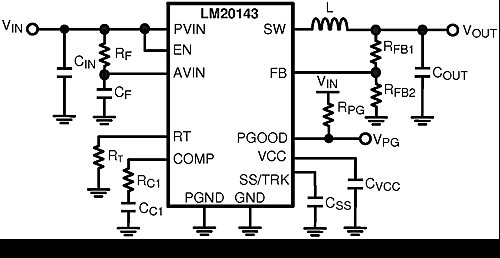 Figure 32. Typical Application Circuit
8.2.1.1 Design Requirements
For this design example, use the parameters listed in Table 1 as the input parameters.
Table 1. Design Parameters
| DESIGN PARAMETER | EXAMPLE VALUE |
|---|---|
| Input voltage range | 3.3 V to 5 V |
| Output voltage | 1.2 V |
| Operating frequency | 1.5 MHz |
| Output current rating | 3 A |
8.2.1.2 Detailed Design Procedure
Table 2 lists components chosen for a circuit design with the listed specifications. The example calculations in this section will use values representative of this circuit design.
Table 2. Bill of Materials
| Designator | Description | Part Number | Manufacturer | Qty |
|---|---|---|---|---|
| U1 | Synchronous Buck Regulator | LM20143 | Texas Instruments | 1 |
| CIN | 47 µF, 1210, X5R, 6.3 V | GRM32ER60J476ME20 | Murata | 1 |
| COUT | 47 µF, 1210, X5R, 6.3 V | GRM32ER60J476ME20 | Murata | 1 |
| L | 1.2 µH, 17 mΩ | DO1813H-122ML | Coilcraft | 1 |
| RPG | 10 kΩ, 0603 | CRCW06031002F-e3 | Vishay-Dale | 1 |
| RF | 1 Ω, 0603 | CRCW06031R0J-e3 | Vishay-Dale | 1 |
| CF | 100 nF, 0603, X7R, 16 V | GRM188R71C104KA01 | Murata | 1 |
| CVCC | 1 µF, 0603, X5R, 6.3 V | GRM188R60J105KA01 | Murata | 1 |
| RC1 | 1 kΩ, 0603 | CRCW06031001F-e3 | Vishay-Dale | 1 |
| CC1 | 4.7 nF, 0603, X7R, 25 V | VJ0603Y472KXXA | Vishay-Vitramon | 1 |
| CSS | 33 nF, 0603, X7R, 25 V | VJ0603Y333KXXA | Vishay-Vitramon | 1 |
| RT | 49.9 kΩ, 0603 | CRCW06034992F-e3 | Vishay-Dale | 1 |
| RFB1 | 4.99 kΩ, 0603 | CRCW06034991F-e3 | Vishay-Dale | 1 |
| RFB2 | 10 kΩ, 0603 | CRCW06031002F-e3 | Vishay-Dale | 1 |
8.2.1.2.1 Duty Cycle Calculation
The first equation to calculate for any buck converter is duty-cycle. Ignoring conduction losses associated with the FETs and parasitic resistances it can be approximated with Equation 3.

The example design the typical duty cycle is calculated to be 66%.
8.2.1.2.2 Inductor Selection (L)
The inductor value is determined based on the operating frequency, load current, ripple current, and duty cycle. To optimize the performance and prevent the device from entering current limit at maximum load, the inductance is typically selected such that the ripple current, ΔiL, is between 25% and 50% of the rated output current. In general, the inductor ripple current, ΔiL, should be greater than 10% of the rated output current to provide adequate current sense information for the current mode control loop. Figure 33 illustrates the switch and inductor ripple current waveforms. Once the input voltage, output voltage, operating frequency, and desired ripple current are known, the minimum value for the inductor can be calculated with Equation 4.

For the example design the calculated inductance is between .405 μH and 0.810 μH.
The inductor selected should have a saturation current rating greater than the peak current limit of the device listed in the Electrical Characteristics table. Keep in mind the specified current limit does not account for delay of the current limit comparator, therefore the current limit in the application may be higher than the specified value. Peak current can be calculated using Equation 5. This value needs to be less than the part current limit threshold. If needed, slightly smaller value inductors can be used, however, the peak inductor current should be kept below the peak current limit of the device.

For the example design the peak inductor current is between 4.563 A and 6.125 A for the selected inductor ripple current range.
Due to exceeding current limit and adding flexibility to accommodate the entire output voltage range a inductance of 1.2 μH was selected, resulting in a peak inductor current of 4.056 A.
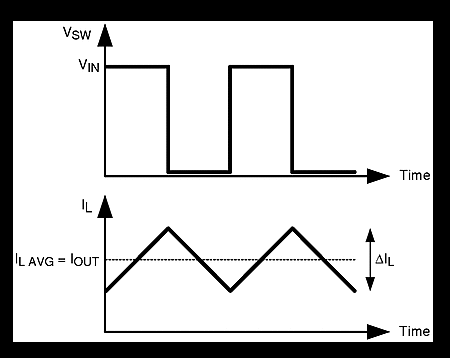 Figure 33. Switch and Inductor Current Waveforms
8.2.1.2.3 Output Capacitor Selection (COUT)
The output capacitor, COUT, filters the inductor ripple current and provides a source of charge for transient load conditions. A wide range of output capacitors may be used with the LM20143 that provide excellent performance. The best performance is typically obtained using ceramic, SP, or OSCON type chemistries. Typical trade-offs are that the ceramic capacitor provides extremely low ESR to reduce the output ripple voltage and noise spikes, while the SP and OSCON capacitors provide a large bulk capacitance in a small volume for transient loading conditions.
When selecting the value for the output capacitor the two performance characteristics to consider are the output voltage ripple and transient response. The output voltage ripple can be approximated by using Equation 6.

where
- ΔVOUT (V) is the amount of peak to peak voltage ripple at the power supply output
- RESR (Ω) is the series resistance of the output capacitor
- fSW(Hz) is the switching frequency
- COUT (F) is the output capacitance used in the design
The amount of output ripple that can be tolerated is application specific; however a general recommendation is to keep the output ripple less than 1% of the rated output voltage. Keep in mind ceramic capacitors are sometimes preferred because they have very low ESR; however, depending on package and voltage rating of the capacitor the value of the capacitance can drop significantly with applied voltage. The output capacitor selection will also affect the output voltage droop during a load transient. The peak droop on the output voltage during a load transient is dependent on many factors; however, an approximation of the transient droop ignoring loop bandwidth can be obtained using Equation 7. Both the tolerance and voltage coefficient of the capacitor needs to be examined when designing for a specific output ripple or transient drop target.

where
- COUT (F) is the minimum required output capacitance
- L (H) is the value of the inductor
- VDROOP (V) is the output voltage drop ignoring loop bandwidth considerations
- ΔIOUTSTEP (A) is the load step change
- RESR (Ω) is the output capacitor ESR
- VIN (V) is the input voltage
- VOUT (V) is the set regulator output voltage
For the example design, a 47-µF ceramic capacitor is selected for the output capacitor to provide good transient and DC performance in a relatively small package. From the technical specifications of this capacitor, the ESR is roughly 3 mΩ, and the effective in-circuit capacitance is approximately 32 µF (reduced from 47 µF due to the 1.2 V DC bias). With these values, the peak-to-peak voltage ripple on the output when operating from a 5-V input can be calculated to be 3 mV. A load transient from 1.5 A to 3 A is calculated to create a 27-mV droop.
8.2.1.2.4 Input Capacitor Selection (CIN)
Good quality input capacitors are necessary to limit the ripple voltage at the VIN pin while supplying most of the switch current during the on-time. In general it is recommended to use a ceramic capacitor for the input as they provide both a low impedance and small footprint. One important note is to use a good dielectric for the ceramic capacitor such as X5R or X7R. These provide better over temperature performance and also minimize the DC voltage derating that occurs on Y5V capacitors. For most applications, a 22-µF, X5R, 6.3-V input capacitor is sufficient; however, additional capacitance may be required if the connection to the input supply is far from the PVIN pins. The input capacitor should be placed as close as possible PVIN and PGND pins of the device.
Non-ceramic input capacitors should be selected for RMS current rating and minimum ripple voltage. A good approximation for the required ripple current rating is given by Equation 8.

As indicated by the RMS ripple current equation, highest requirement for RMS current rating occurs at 50% duty cycle. For this case, the RMS ripple current rating of the input capacitor should be greater than half the output current. For best performance, low ESR ceramic capacitors should be placed in parallel with higher capacitance capacitors to provide the best input filtering for the device.
For the example design the rated RMS current must be at least 1.5 A. A 47-µF ceramic capacitor provides the necessary input capacitance for the evaluation board. For improved bypassing, a small 1-µF high frequency capacitor is placed in parallel with the 47-µF bulk capacitor to filter high frequency noise pulses on the supply.
8.2.1.2.5 Setting the Output Voltage (RFB1, RFB2)
The resistors RFB1 and RFB2 are selected to set the output voltage for the device. For most applications, RFB1 should be between 4.99 kΩ to 49.9 kΩ.

For the example design RFB1 = 4 kΩ and RFB2 = 10 kΩ to set the output voltage at 1.2 V.
Table 3 contains common output voltage values for RFB1 and RFB2.
Table 3. Suggested Values for RFB1 and RFB2
| RFB1(kΩ) | RFB2(kΩ) | VOUT |
|---|---|---|
| short | open | 0.8 |
| 4.99 | 10 | 1.2 |
| 8.87 | 10.2 | 1.5 |
| 12.7 | 10.2 | 1.8 |
| 21.5 | 10.2 | 2.5 |
| 31.6 | 10.2 | 3.3 |
8.2.1.2.6 Adjusting the Operating Frequency (RT)
The LM20143 supports a wide range of switching frequencies from 500 kHz to 1.5 MHz. The operating frequency of the LM20143 can be adjusted by connecting a resistor from the RT pin to ground. The choice of switching frequency is usually a compromise between efficiency and the size of the circuit. Lower switching frequency implies reduced switching losses, usually resulting in higher overall efficiency. However, higher switching frequency allows use of smaller inductor and output capacitor components, resulting in a smaller design. The optimal switching frequency is usually a tradeoff in a given application and thus should be determined on a case-by-case basis. For the design example a relatively high switching frequency was selected to minimize circuit size. Equation 10 can be used to calculate the value of RT for a given operating frequency.

where
- fSW is the switching frequency in kHz
- RT is the frequency adjust resistor in kΩ
Please refer to the curve Oscillator Frequency verses RT in the typical performance characteristics section. If the RT resistor is omitted the device will not operate.
For the example design RT was calculated to be 49.9 kΩ to give a switching frequency of 1.5 MHz.
8.2.1.2.7 AVIN Filtering Components (CF and RF)
To prevent high frequency noise spikes from disturbing the sensitive analog circuitry connected to the AVIN and AGND pins, a high frequency RC filter is required between PVIN and AVIN. These components are shown in Figure 32 as CF and RF. The required value for RF is 1 Ω. CF must be used. Recommended value of CF is 1.0 µF. The filter capacitor, CF should be placed as close to the IC as possible with a direct connection from AVIN to AGND. A good quality X5R or X7R ceramic capacitor should be used for CF.
For the example design, RF 1 Ω and CF is 1.0 µF, providing greater than 16 dB of attenuation at the set 1.5-MHz switching frequency.
8.2.1.2.8 Sub-Regulator Bypass Capacitor (CVCC)
The capacitor at the VCC pin provides noise filtering and stability for the internal sub-regulator. The recommended value of CVCC should be no smaller than 1 µF and no greater than 10 µF. The capacitor should be a good quality ceramic X5R or X7R capacitor. In general, a 1-µF ceramic capacitor is recommended for most applications. In the example design, CVCC is 1 µF.
8.2.1.2.9 Setting the Start Up Time (CSS)
The addition of a capacitor connected from the SS pin to ground sets the time at which the output voltage will reach the final regulated value. Larger values for CSS will result in longer start up times. While the Soft-Start capacitor can be sized to meet many start up requirements, there are limitations to its size. The Soft-Start time can never be faster than 1 ms due to the internal default 1-ms start up time. When the device is enabled there is an approximate time interval of 50 μs when the Soft-Start capacitor will be discharged just prior to the Soft-Start ramp. If the enable pin is rapidly pulsed or the Soft-Start capacitor is large there may not be enough time for CSS to completely discharge resulting in start up times less than predicted. To aid in discharging of Soft-Start capacitor during long disable periods an external 1-MΩ resistor from SS/TRK to ground can be used without greatly affecting the start up time. Equation 11 can be used to calculate the desired soft start time. For the LM20143, ISS is nominally 5 µA, that may be found in the electrical characteristics table.

For the example design the start-up time was set to be around 5ms resulting in a 33 nF capacitor.
Table 4 shows values of CSS for some common start up times.
Table 4. Start Up Times for Different Soft-Start Capacitors
| Start Up Time (ms) | CSS (nF) |
|---|---|
| 1 | none |
| 5 | 33 |
| 10 | 68 |
| 15 | 100 |
| 20 | 120 |
8.2.1.2.10 Loop Compensation (RC1, CC1)
The purpose of loop compensation is to meet static and dynamic performance requirements while maintaining adequate stability. Optimal loop compensation depends on the output capacitor, inductor, load, and the device itself. Table 5 gives values for the compensation network that will result in a stable system when using a 100-µF, 6.3-V ceramic X5R output capacitor and 1-µH inductor.
Table 5. Recommended Compensation for COUT = 100 µF, L = 1 µH & fSW = 1 MHz
| VIN | VOUT | CC1 (nF) | RC1 (kΩ) |
|---|---|---|---|
| 5.00 | 3.30 | 4.7 | 17.8 |
| 5.00 | 2.50 | 4.7 | 12.1 |
| 5.00 | 1.80 | 4.7 | 7.68 |
| 5.00 | 1.50 | 4.7 | 5.9 |
| 5.00 | 1.20 | 4.7 | 3.57 |
| 5.00 | 0.80 | 4.7 | 1.58 |
| 3.30 | 2.50 | 4.7 | 13 |
| 3.30 | 1.80 | 4.7 | 9.76 |
| 3.30 | 1.50 | 4.7 | 6.49 |
| 3.30 | 1.20 | 4.7 | 4.64 |
| 3.30 | 0.80 | 4.7 | 1.58 |
If the desired solution differs from those provided, the loop transfer function should be analyzed to optimize the loop compensation. The overall loop transfer function is the product of the power stage and the feedback network transfer functions. For stability purposes, the objective is to have a loop gain slope that is –20 db/decade from a very low frequency to beyond the crossover frequency. Figure 34 shows the transfer functions for power stage, feedback/compensation network, and the resulting closed loop system for the LM20143.
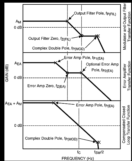 Figure 34. LM20143 Loop Compensation
The power stage transfer function is dictated by the modulator, output LC filter, and load; while the feedback transfer function is set by the feedback resistor ratio, error amp gain, and external compensation network.
To achieve a –20 dB/decade slope, the error amplifier zero, located at fZ(EA), should positioned to cancel the output filter pole (fP(FIL)). An additional error amp pole, located at fP2(EA), can be added to cancel the output filter zero at fZ(FIL). Cancellation of the output filter zero is recommended if larger value, non-ceramic output capacitors are used.
Compensation of the LM20143 is achieved by adding an RC network as shown in Figure 35.
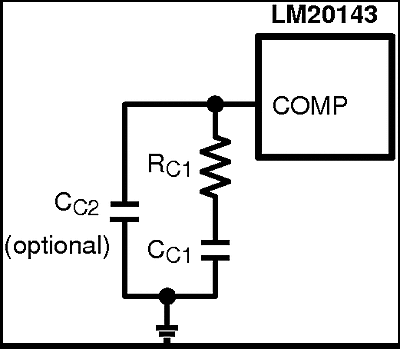 Figure 35. Compensation Network for LM20143
A good starting value for CC1 for most applications is 4.7 nF. Once the value of CC1 is chosen the value of RC should be calculated using Equation 12 to cancel the output filter pole (fP(FIL)) as shown in Figure 34.

A higher crossover frequency can be obtained, usually at the expense of phase margin, by lowering the value of CC1 and recalculating the value of RC1. Likewise, increasing CC1 and recalculating RC1 will provide additional phase margin at a lower crossover frequency. As with any attempt to compensate the LM20143 the stability of the system should be verified for desired transient droop and settling time.
If the output filter zero, fZ(FIL) approaches the crossover frequency (FC), an additional capacitor (CC2) should be placed at the COMP pin to ground. This capacitor adds a pole to cancel the output filter zero assuring the crossover frequency will occur before the double pole at fSW / 2 degrades the phase margin. The output filter zero is set by the output capacitor value and ESR as shown in Equation 13.

If needed, the value for CC2 should be calculated using Equation 14.

where
- RESR is the output capacitor series resistance
- RC1 is the calculated compensation resistance
For the example design RC1 is 1 kΩ, CC1 is 4.7 nF and CC2is left open.
8.2.1.3 Application Curves
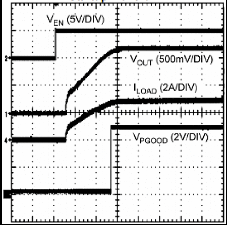
| VIN = 5 V | VOUT = 1.2 V | IOUT = 3 A |
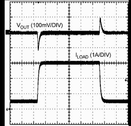
| VIN = 5 V | VOUT = 1.2 V | IOUT = 0.5 A to 3 A |
| Time Scale = 200 µs/div | ||
8.2.2 5-V Supply Rail Design
 Figure 38. Typical Application Circuit
8.2.2.1 Design Requirements
For this design example, use the parameters listed in Table 6 as the input parameters.
Table 6. Design Parameters
| DESIGN PARAMETER | EXAMPLE VALUE |
|---|---|
| Input voltage range | 5 V |
| Output voltage | 3.3 V |
| Operating frequency | 750 kHz |
| Output current rating | 3 A |
8.2.2.2 Detailed Design Procedure
Table 7 lists a selection of components using the design procedure explained in 3.3-V or 5-V Supply Rail Design for a circuit design with the listed specifications.
Table 7. Bill of Materials
| Designator | Description | Part Number | Manufacturer | Qty |
|---|---|---|---|---|
| U1 | Synchronous Buck Regulator | LM20143 | Texas Instruments | 1 |
| CIN | 47 µF, 1210, X5R, 6.3 V | GRM32ER60J476ME20 | Murata | 1 |
| COUT | 100 µF, 1210, X5R, 6.3 V | GRM32ER60J107ME20 | Murata | 1 |
| L | 1.5 µH, 8.1 mΩ | MSS1038-152NL | Coilcraft | 1 |
| RF | 1 Ω, 0603 | CRCW06031R0J-e3 | Vishay-Dale | 1 |
| CF | 100 nF, 0603, X7R, 16 V | GRM188R71C104KA01 | Murata | 1 |
| CVCC | 1 µF, 0603, X5R, 6.3 V | GRM188R60J105KA01 | Murata | 1 |
| RC1 | 10 kΩ, 0603 | CRCW06031002F-e3 | Vishay-Dale | 1 |
| CC1 | 3.3 nF, 0603, X7R, 25 V | VJ0603Y332KXXA | Vishay-Vitramon | 1 |
| CSS | 33 nF, 0603, X7R, 25 V | VJ0603Y333KXXA | Vishay-Vitramon | 1 |
| RT | 150 kΩ, 0603 | CRCW06031503F-e3 | Vishay-Dale | 1 |
| RFB1 | 31.6 kΩ, 0603 | CRCW06033162F-e3 | Vishay-Dale | 1 |
| RFB2 | 10.2 kΩ, 0603 | CRCW06031022F-e3 | Vishay-Dale | 1 |
8.2.3 3-V Supply Rail Design
 Figure 39. Typical Application Circuit
8.2.3.1 Design Requirements
For this design example, use the parameters listed in Table 8 as the input parameters.
Table 8. Design Parameters
| DESIGN PARAMETER | EXAMPLE VALUE |
|---|---|
| Input voltage range | 3.3 V |
| Output voltage | 1.2 V |
| Operating frequency | 750 kHz |
| Output current rating | 3 A |
8.2.3.2 Detailed Design Procedure
Table 9 lists a selection of components using the design procedure explained in 3.3-V or 5-V Supply Rail Design for a circuit design with the listed specifications.
Table 9. Bill of Materials
| Designator | Description | Part Number | Manufacturer | Qty |
|---|---|---|---|---|
| U1 | Synchronous Buck Regulator | LM20143 | Texas Instruments | 1 |
| CIN | 47 µF, 1210, X5R, 6.3 V | GRM32ER60J476ME20 | Murata | 1 |
| COUT | 100 µF, 1210, X5R, 6.3 V | GRM32ER60J107ME20 | Murata | 1 |
| L | 1.2 µH, 17 mΩ | DO1813H-122ML | Coilcraft | 1 |
| RF | 1 Ω, 0603 | CRCW06031R0J-e3 | Vishay-Dale | 1 |
| CF | 100 nF, 0603, X7R, 16 V | GRM188R71C104KA01 | Murata | 1 |
| CVCC | 1 µF, 0603, X5R, 6.3 V | GRM188R60J105KA01 | Murata | 1 |
| RC1 | 2 kΩ, 0603 | CRCW06032001F-e3 | Vishay-Dale | 1 |
| CC1 | 4.7 nF, 0603, X7R, 25 V | VJ0603Y472KXXA | Vishay-Vitramon | 1 |
| CSS | 33 nF, 0603, X7R, 25 V | VJ0603Y333KXXA | Vishay-Vitramon | 1 |
| RT | 150 kΩ, 0603 | CRCW06031503F-e3 | Vishay-Dale | 1 |
| RFB1 | 4.99 kΩ, 0603 | CRCW06034991F-e3 | Vishay-Dale | 1 |
| RFB2 | 10 kΩ, 0603 | CRCW06031002F-e3 | Vishay-Dale | 1 |