SNVS528H October 2007 – January 2016 LM20143 , LM20143-Q1
PRODUCTION DATA.
- 1 Features
- 2 Applications
- 3 Description
- 4 Revision History
- 5 Pin Configuration and Functions
- 6 Specifications
- 7 Detailed Description
-
8 Application and Implementation
- 8.1 Application Information
- 8.2
Typical Applications
- 8.2.1
3.3-V or 5-V Supply Rail Design
- 8.2.1.1 Design Requirements
- 8.2.1.2
Detailed Design Procedure
- 8.2.1.2.1 Duty Cycle Calculation
- 8.2.1.2.2 Inductor Selection (L)
- 8.2.1.2.3 Output Capacitor Selection (COUT)
- 8.2.1.2.4 Input Capacitor Selection (CIN)
- 8.2.1.2.5 Setting the Output Voltage (RFB1, RFB2)
- 8.2.1.2.6 Adjusting the Operating Frequency (RT)
- 8.2.1.2.7 AVIN Filtering Components (CF and RF)
- 8.2.1.2.8 Sub-Regulator Bypass Capacitor (CVCC)
- 8.2.1.2.9 Setting the Start Up Time (CSS)
- 8.2.1.2.10 Loop Compensation (RC1, CC1)
- 8.2.1.3 Application Curves
- 8.2.2 5-V Supply Rail Design
- 8.2.3 3-V Supply Rail Design
- 8.2.1
3.3-V or 5-V Supply Rail Design
- 9 Power Supply Recommendations
- 10Layout
- 11Device and Documentation Support
- 12Mechanical, Packaging, and Orderable Information
6 Specifications
6.1 Absolute Maximum Ratings
See (1)| MIN | MAX | UNIT | ||
|---|---|---|---|---|
| AVIN, PVIN, EN, PGOOD, SS/TRK, COMP, FB, RT | Voltages from indicated pins to GND | –0.3 | 6 | V |
| Power Dissipation(2) | 2.6 | W | ||
| Junction Temperature | 150 | °C | ||
| Lead Temperature (Soldering, 10 sec) | 260 | °C | ||
| Storage Temperature | –65 | 150 | °C | |
(1) Stresses beyond those listed under Absolute Maximum Ratings may cause permanent damage to the device. These are stress ratings only, which do not imply functional operation of the device at these or any other conditions beyond those indicated under Recommended Operating Conditions. Exposure to absolute-maximum-rated conditions for extended periods may affect device reliability.
(2) The maximum allowable power dissipation is a function of the maximum junction temperature, TJ_MAX, the junctions-to-ambient thermal resistance, θJA, and the ambient temperature, TA. The maximum allowable power dissipation at any ambient temperature is calculated using: PD_MAX = (TJ_MAX – TA) / θJA. The maximum power dissipations of 2.6 W is determined using TA = 25°C, θJA = 38°C/W, and TJ_MAX = 125°C.
6.2 ESD Ratings
| VALUE | UNIT | |||
|---|---|---|---|---|
| V(ESD) | Electrostatic discharge | Human-body model (HBM), per ANSI/ESDA/JEDEC JS-001(1) | ±2000 | V |
| Charged-device model (CDM), per JEDEC specification JESD22-C101(2) | ±1000 | |||
(1) JEDEC document JEP155 states that 500-V HBM allows safe manufacturing with a standard ESD control process.
(2) JEDEC document JEP157 states that 250-V CDM allows safe manufacturing with a standard ESD control process.
6.3 Recommended Operating Conditions
| MIN | MAX | UNIT | |
|---|---|---|---|
| PVIN, AVIN to GND | 2.95 | 5.5 | V |
| Junction Temperature | −40 | 125 | °C |
6.4 Thermal Information
| THERMAL METRIC(1) | LM20143 | UNIT | |
|---|---|---|---|
| PWP (HTSSOP) | |||
| 16 PINS | |||
| RθJA | Junction-to-ambient thermal resistance (2) | 39.3 | °C/W |
| RθJC(top) | Junction-to-case (top) thermal resistance (3) | 20.3 | °C/W |
| RθJB | Junction-to-board thermal resistance | 9.9 | °C/W |
| ψJT | Junction-to-top characterization parameter | 0.6 | °C/W |
| ψJB | Junction-to-board characterization parameter | 9.9 | °C/W |
| RθJC(bot) | Junction-to-case (bottom) thermal resistance | 12.1 | °C/W |
(1) For more information about traditional and new thermal metrics, see the Semiconductor and IC Package Thermal Metrics application report, SPRA953.
(2) On JEDEC 4-Layer test board (JESD 51-7) with eight (8) thermal vias.
(3) θJC refers to center of the Exposed Pad on the bottom of the package as the case.
6.5 Electrical Characteristics
Unless otherwise stated, the following conditions apply: AVIN = PVIN = VIN = 5 V. All Typical limits are for TJ = 25°C only, all Minimum and Maximum limits apply over the junction temperature (TJ) range of –40°C to 125°C(1). Typical values represent the most likely parametric norm at TJ = 25°C, and are provided for reference purposes only.| PARAMETER | TEST CONDITIONS | MIN | TYP | MAX | UNIT | |
|---|---|---|---|---|---|---|
| VFB | Feedback pin voltage | VIN = 2.95 V to 5.5 V | 0.788 | 0.8 | 0.812 | V |
| ΔVOUT/ΔIOUT | Load Regulation | IOUT = 100 mA to 3 A | 0.08 | %/A | ||
| ICL | Switch Current Limit Threshold | VIN = 3.3 V | 4.3 | 4.8 | 5.3 | A |
| RDS_ON | High-Side Switch On Resistance | ISW = 3.5 A | 36 | 55 | mΩ | |
| RDS_ON | Low-Side Switch On Resistance | ISW = 3.5 A | 32 | 52 | mΩ | |
| IQ | Operating Quiescent Current | Non-switching, VFB = VCOMP | 3.5 | 6 | mA | |
| ISD | Shutdown Quiescent current | VEN = 0 V | 90 | 180 | µA | |
| VUVLO | VIN Under Voltage Lockout | Rising VIN | 2.45 | 2.7 | 2.95 | V |
| VUVLO_HYS | VIN Under Voltage Lockout Hysteresis | Falling VIN | 45 | 100 | mV | |
| VVCC | VCC Voltage | IVCC = 0 µA | 2.45 | 2.7 | 2.95 | V |
| ISS | Soft-Start Pin Source Current | VSS/TRK = 0 V | 2 | 4.5 | 7 | µA |
| VTRACK | SS/TRK Accuracy, VSS - VFB | VSS/TRK = 0.4 V | –10 | 3 | 15 | mV |
| OSCILLATOR | ||||||
| FOSCH | Oscillator Frequency | RT = 49.9 kΩ | 1350 | 1500 | 1650 | kHz |
| FOSCL | Oscillator Frequency | RT = 249 kΩ | 450 | 510 | 570 | kHz |
| DCMAX | Maximum Duty Cycle | ILOAD = 0 A | 85% | |||
| TON_TIME | Minimum On Time | 100 | ns | |||
| TCL_BLANK | Current Sense Blanking Time | After Rising VSW | 80 | ns | ||
| ERROR AMPLIFIER AND MODULATOR | ||||||
| IFB | Feedback pin bias current | VFB = 0.8 V | 1 | 100 | nA | |
| ICOMP_SRC | COMP Output Source Current | VFB = VCOMP = 0.6 V | 80 | 100 | µA | |
| ICOMP_SNK | COMP Output Sink Current | VFB = 1.0 V, VCOMP = 0.6 V | 80 | 100 | µA | |
| Gm | Error Amplifier Transconductance | ICOMP = ± 50 µA | 450 | 510 | 600 | µmho |
| AVOL | Error Amplifier Voltage Gain | 2000 | V/V | |||
| POWER GOOD | ||||||
| VOVP | Over Voltage Protection Rising Threshold | With respect to VFB | 105% | 108% | 111% | |
| VOVP_HYS | Over Voltage Protection Hysteresis | With respect to VFB | 2% | 3% | ||
| VPGTH | PGOOD Rising Threshold | With respect to VFB | 92% | 94% | 96% | |
| VPGHYS | PGOOD Falling Hysteresis | With respect to VFB | 2% | 3% | ||
| TPGOOD | PGOOD deglitch time | 16 | µs | |||
| IOL | PGOOD Low Sink Current | VPGOOD = 0.4 V | 0.6 | 1 | mA | |
| IOH | PGOOD High Leakage Current | VPGOOD = 5 V | 5 | 100 | nA | |
| ENABLE | ||||||
| VIH_EN | EN Pin turn-on Threshold | VEN Rising | 1.08 | 1.18 | 1.28 | V |
| VEN_HYS | EN Pin Hysteresis | 66 | mV | |||
| THERMAL SHUTDOWN | ||||||
| TSD | Thermal Shutdown | 160 | °C | |||
| TSD_HYS | Thermal Shutdown Hysteresis | 10 | °C | |||
(1) Minimum and Maximum limits are specified by test, design, or statistical correlation.
6.6 Typical Characteristics
Unless otherwise specified: CIN = COUT = 100 µF, L = 1.0 µH, VIN = 5 V, VOUT = 1.2 V, RLOAD = 1.2 Ω, fSW = 1 MHz, TA = 25°C for efficiency curves, loop gain plots and waveforms, and TJ = 25°C for all others.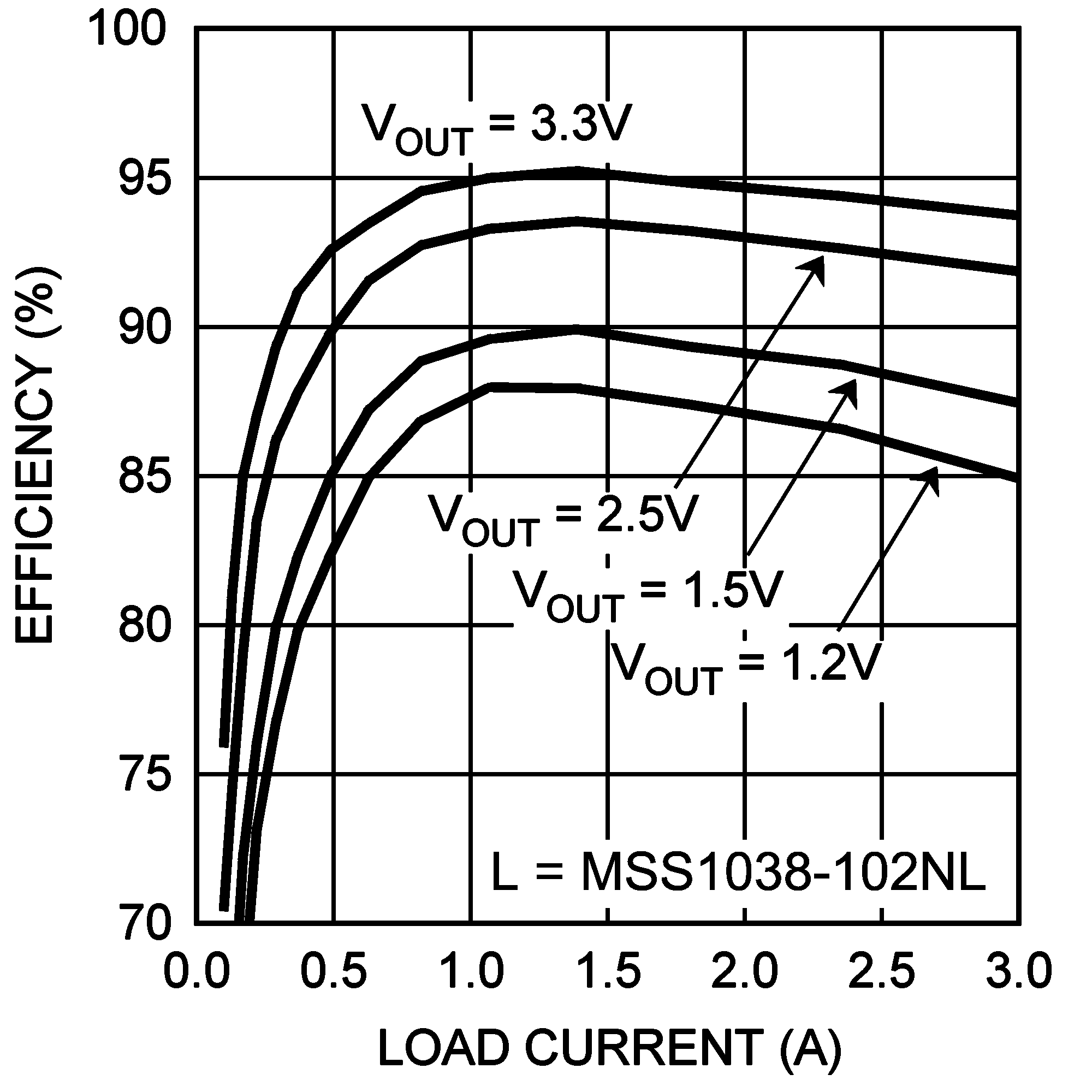
| VIN = 5 V | fSW = 1.5 MHz |
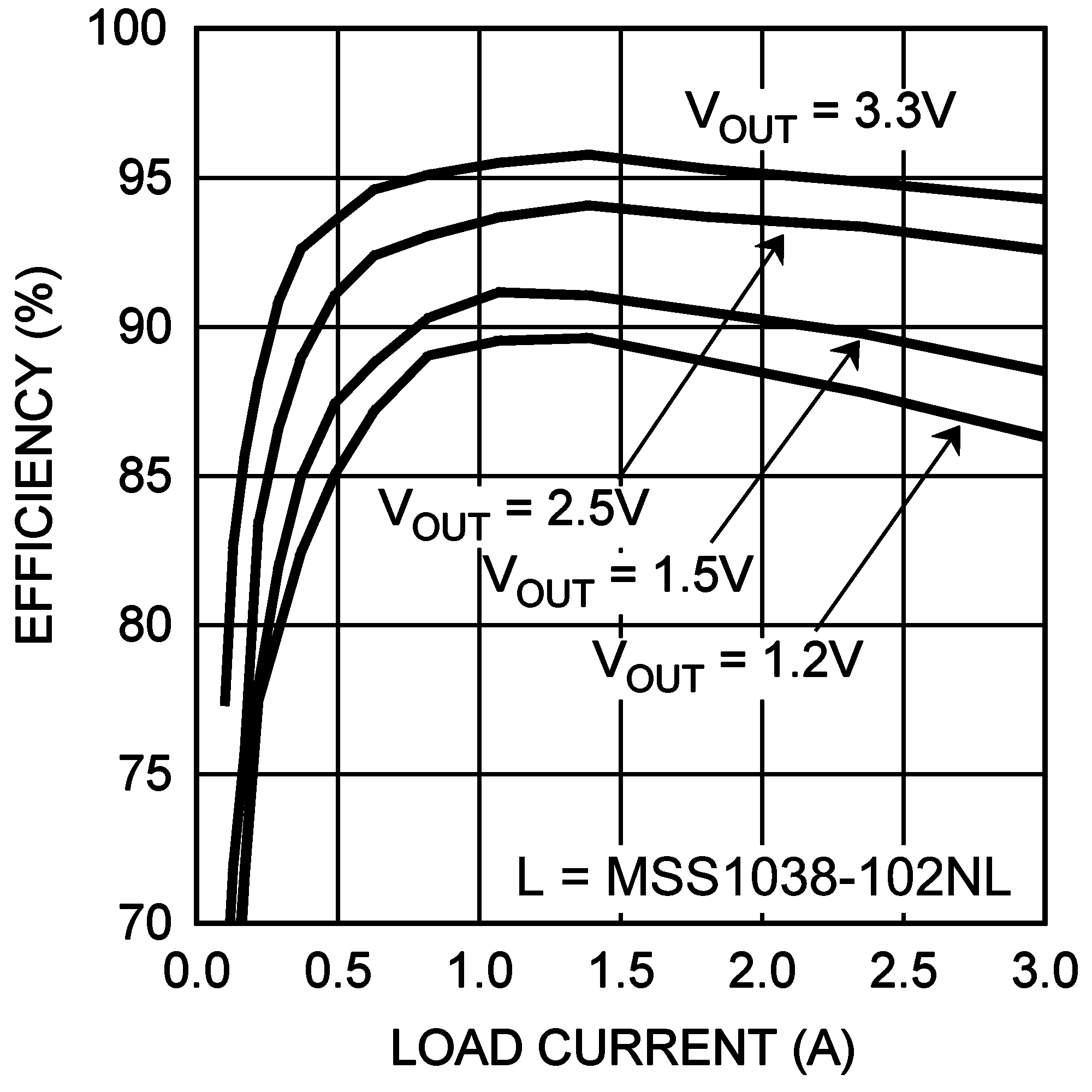
| VIN = 5 V | fSW = 1.0 MHz |
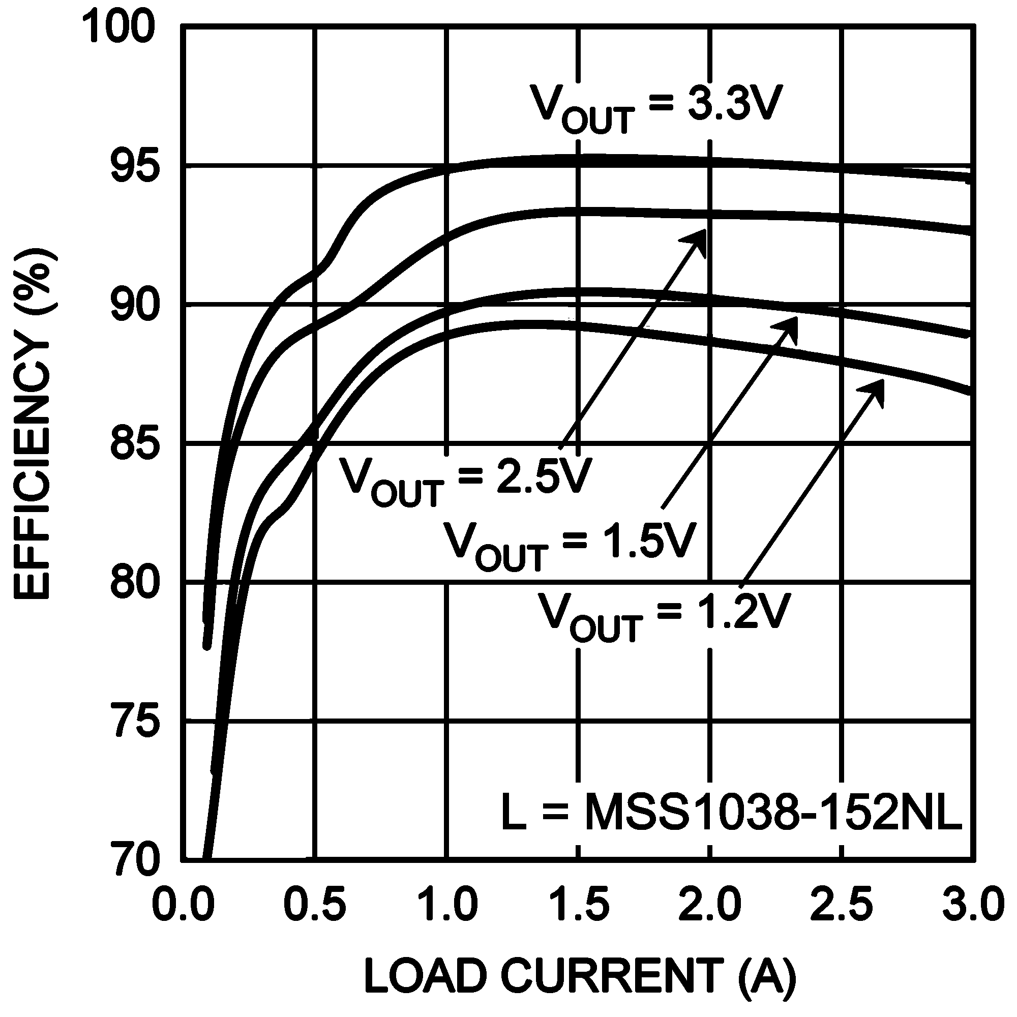
| VIN = 5.0 V | fSW 500 kHz |
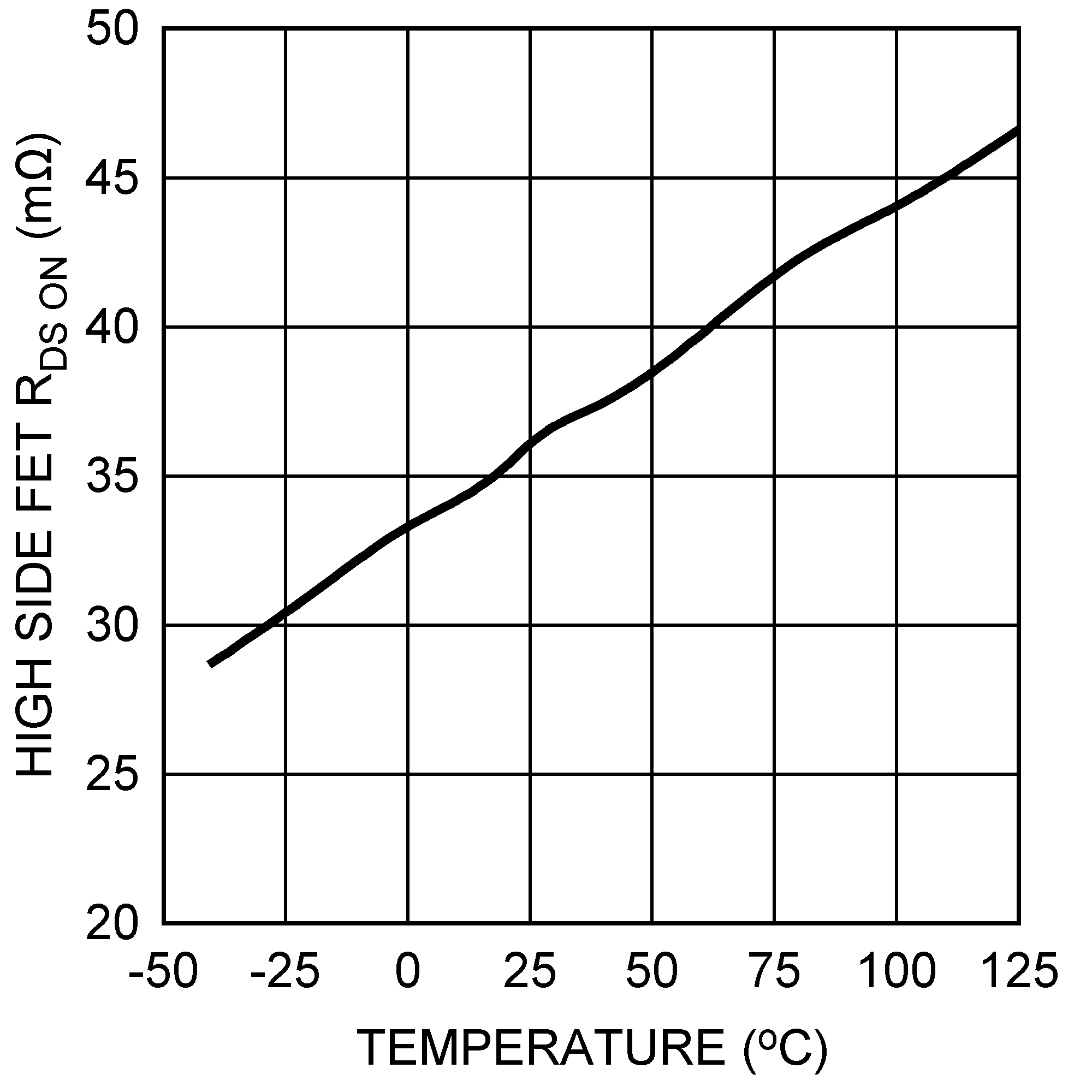 Figure 7. High-Side FET Resistance vs Temperature
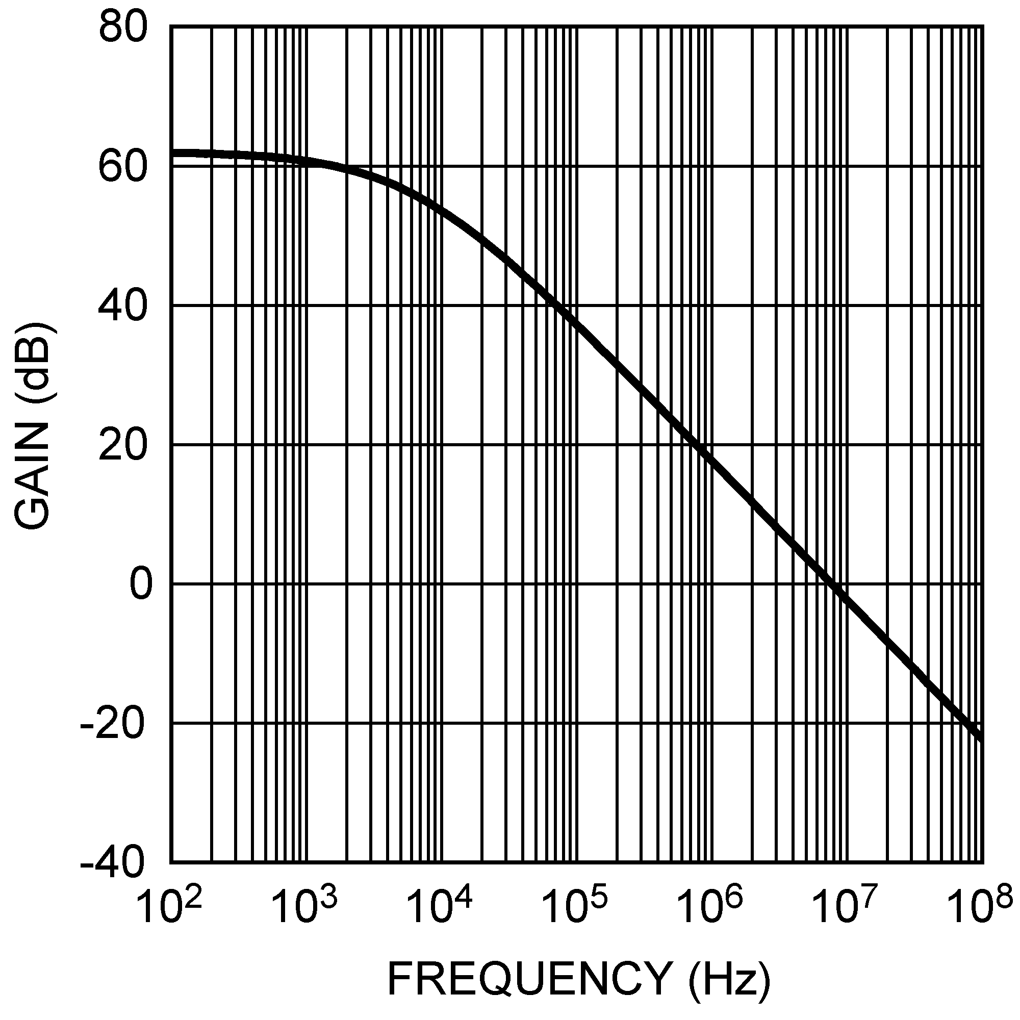 Figure 9. Error Amplifier Gain vs Frequency
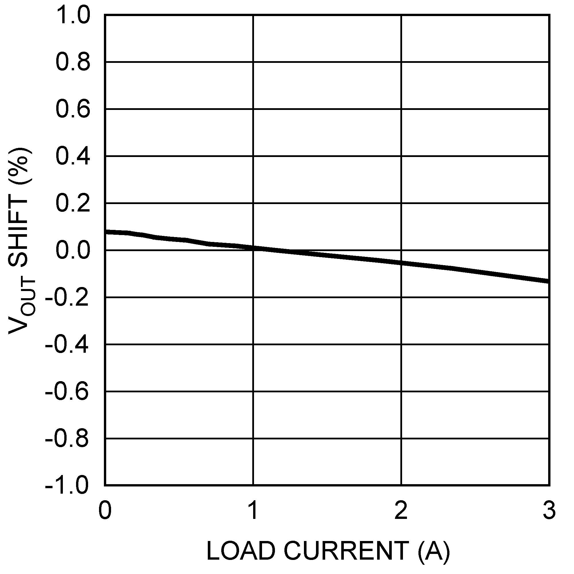 Figure 11. Load Regulation
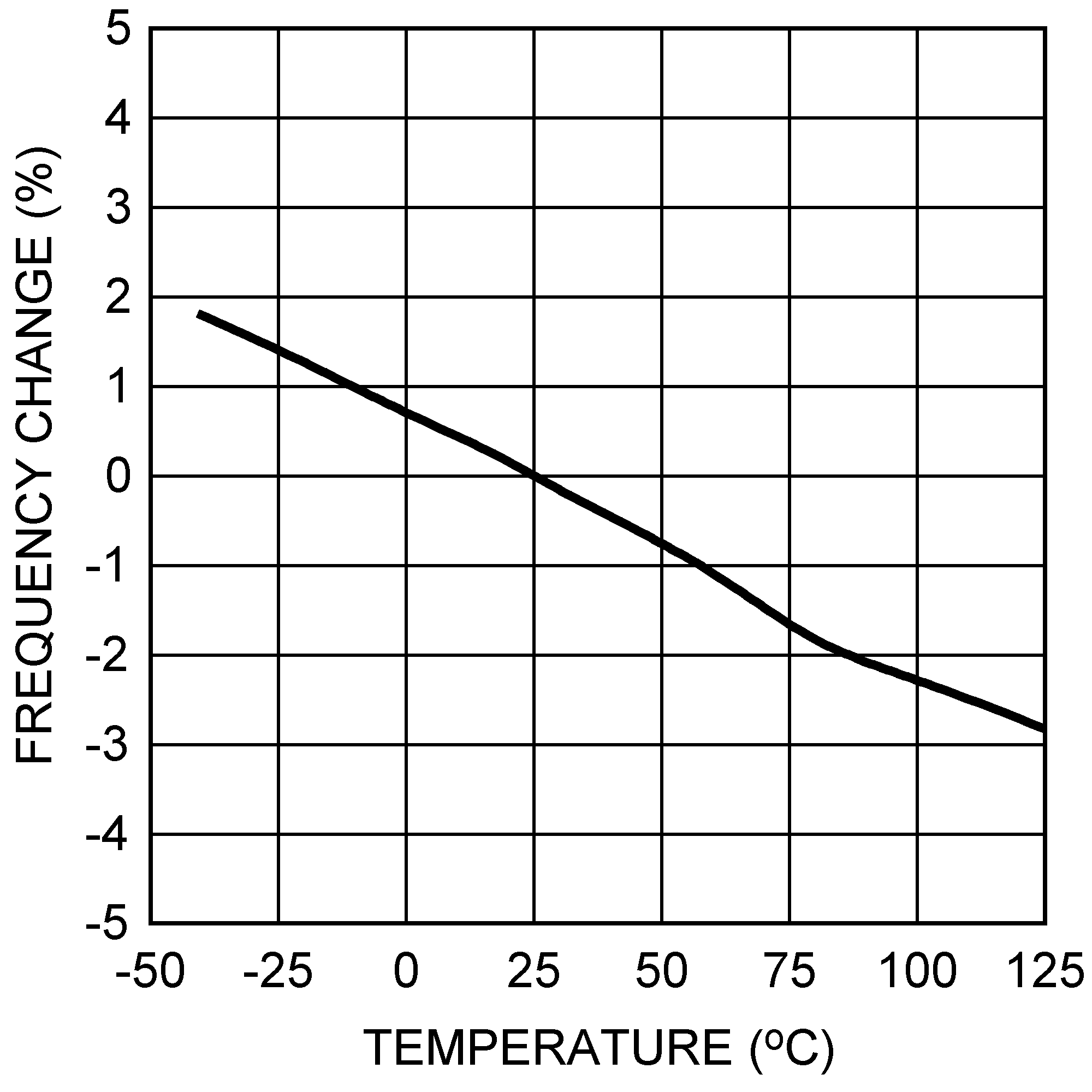 Figure 13. Switching Frequency vs Temperature
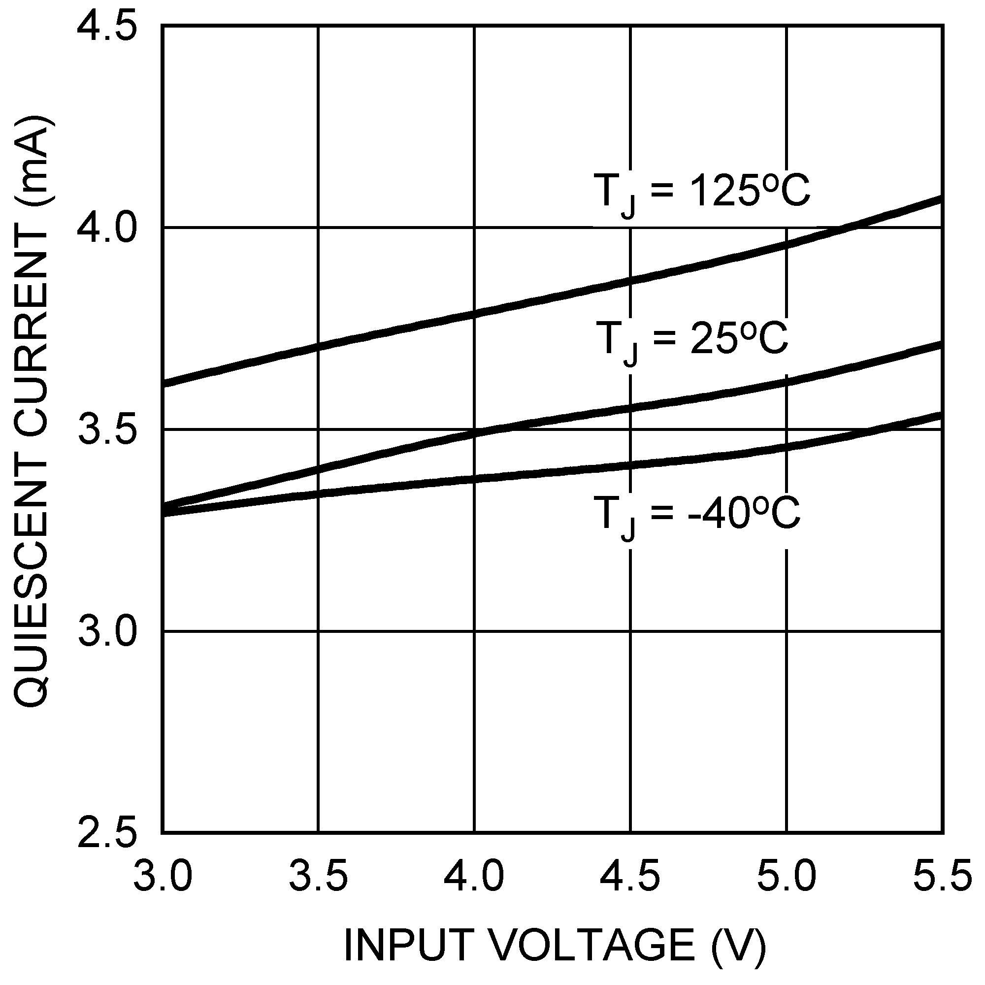 Figure 15. Quiescent Current vs VIN (Not Switching)
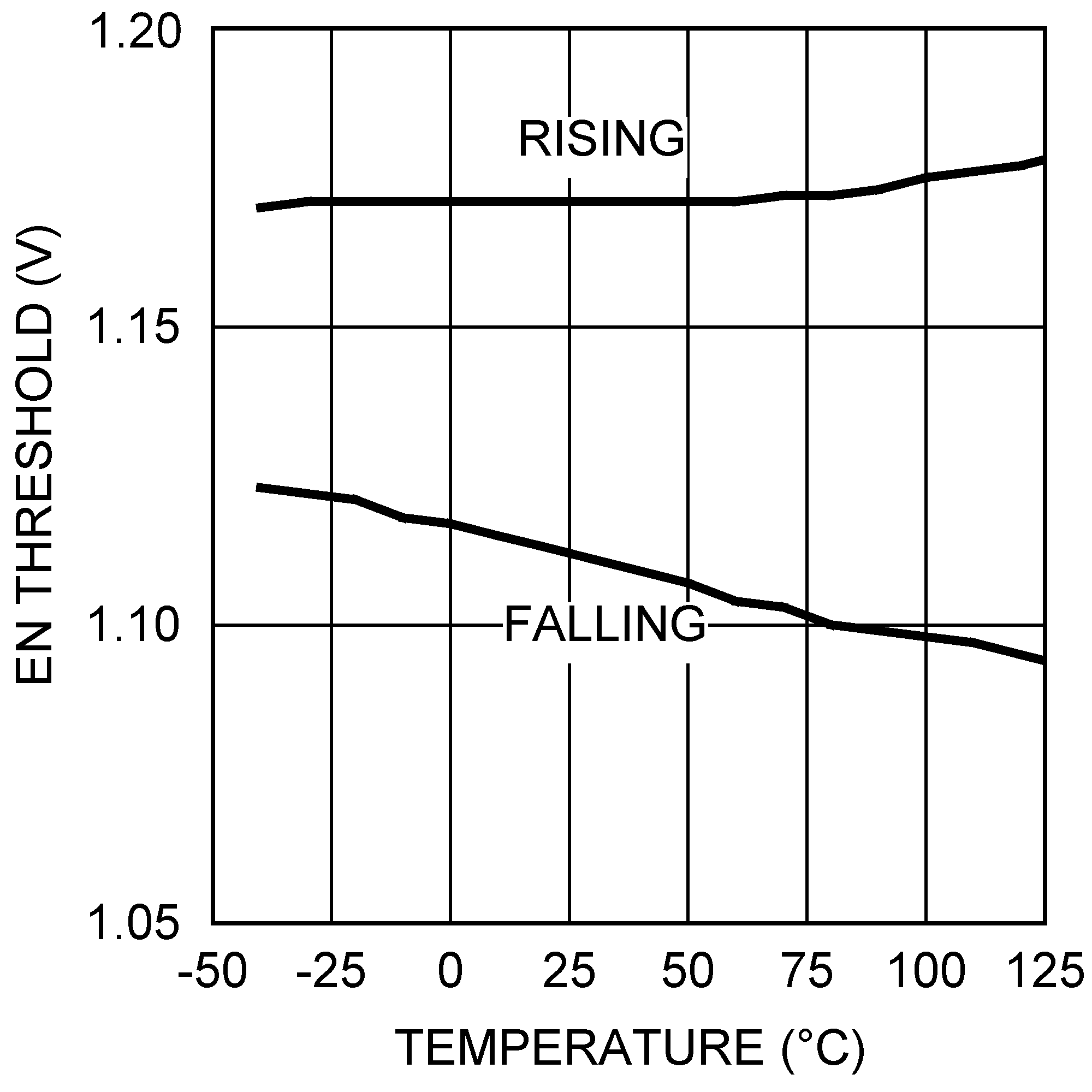 Figure 17. Enable Threshold vs Temperature
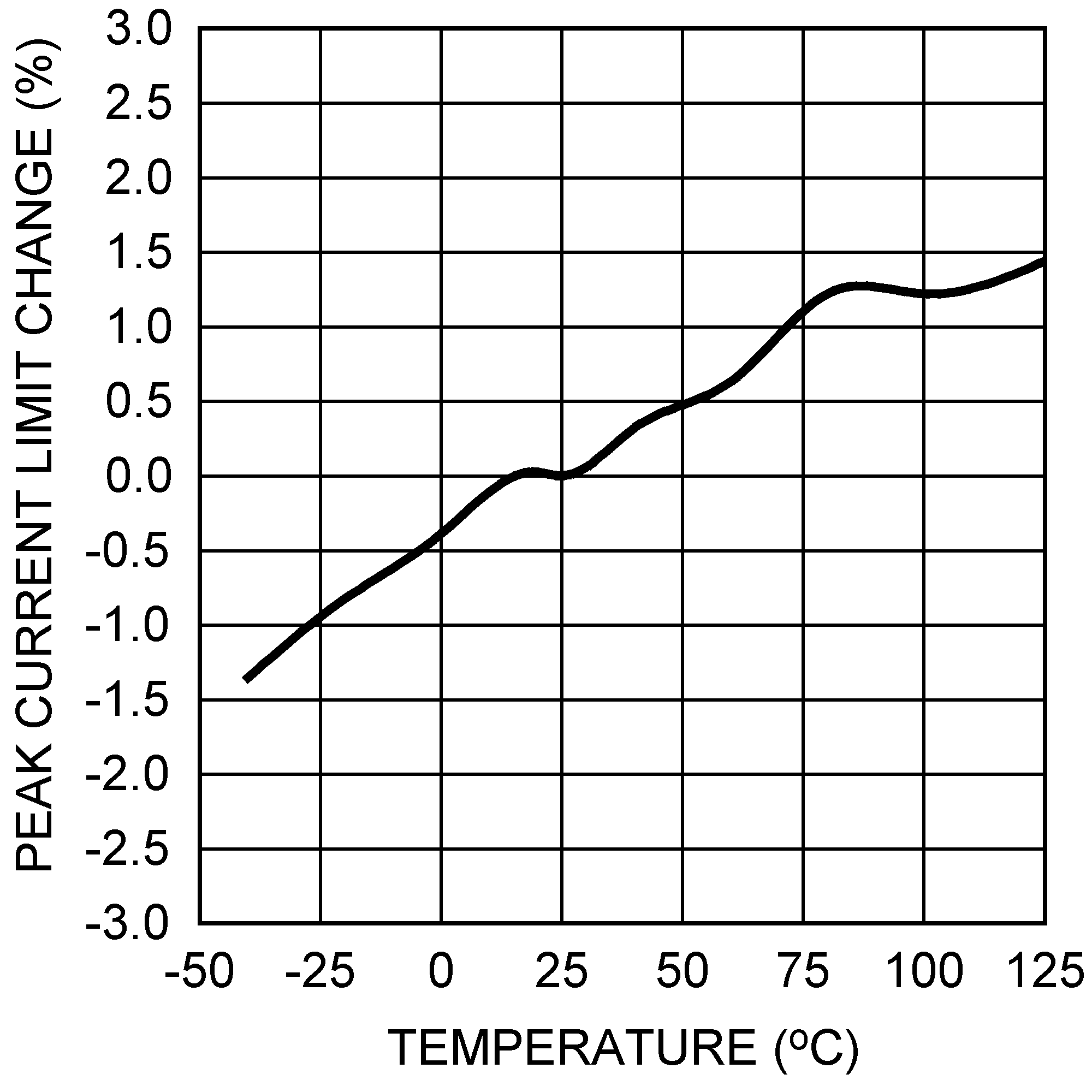 Figure 19. Peak Current Limit vs Temperature
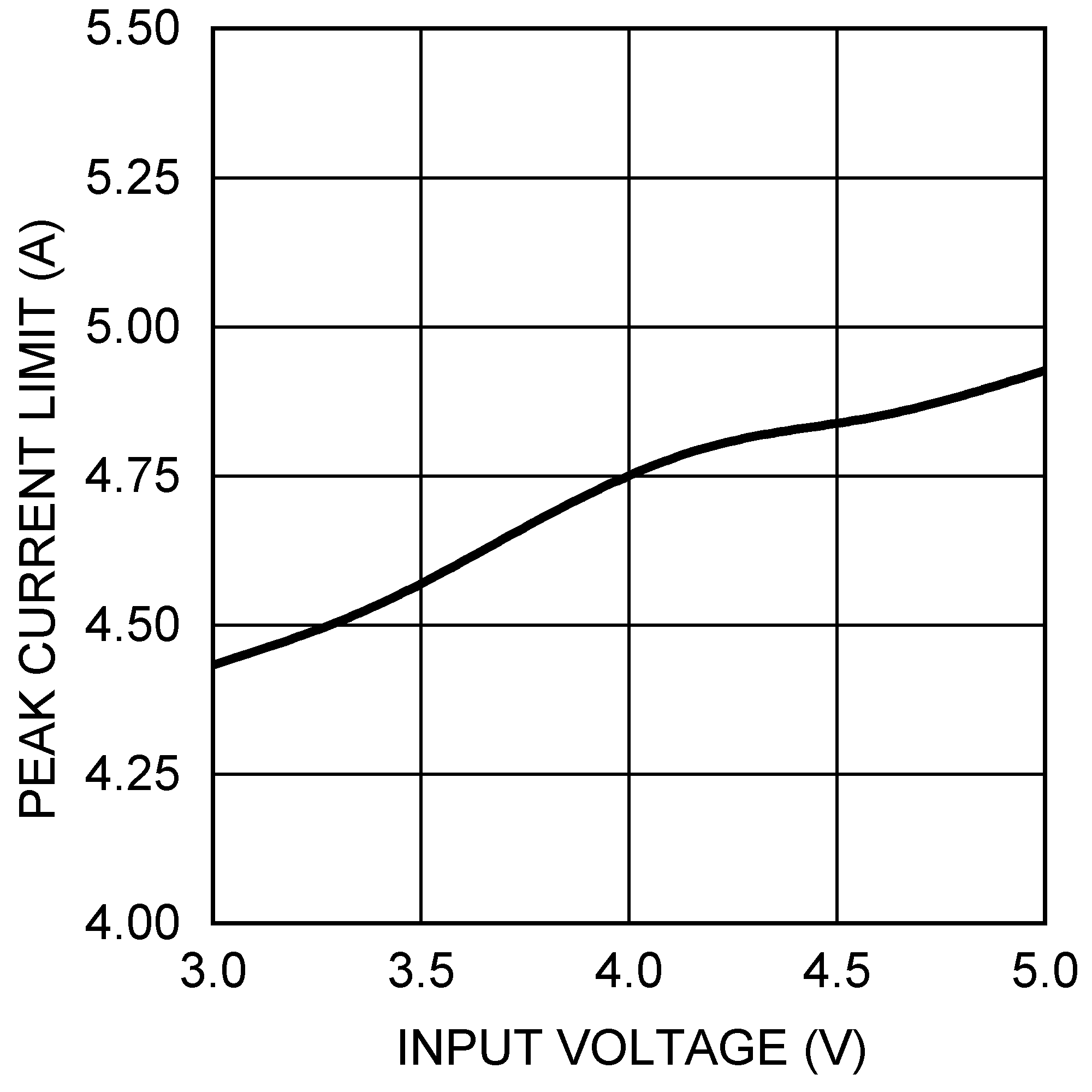 Figure 21. Peak Current Limit vs VIN
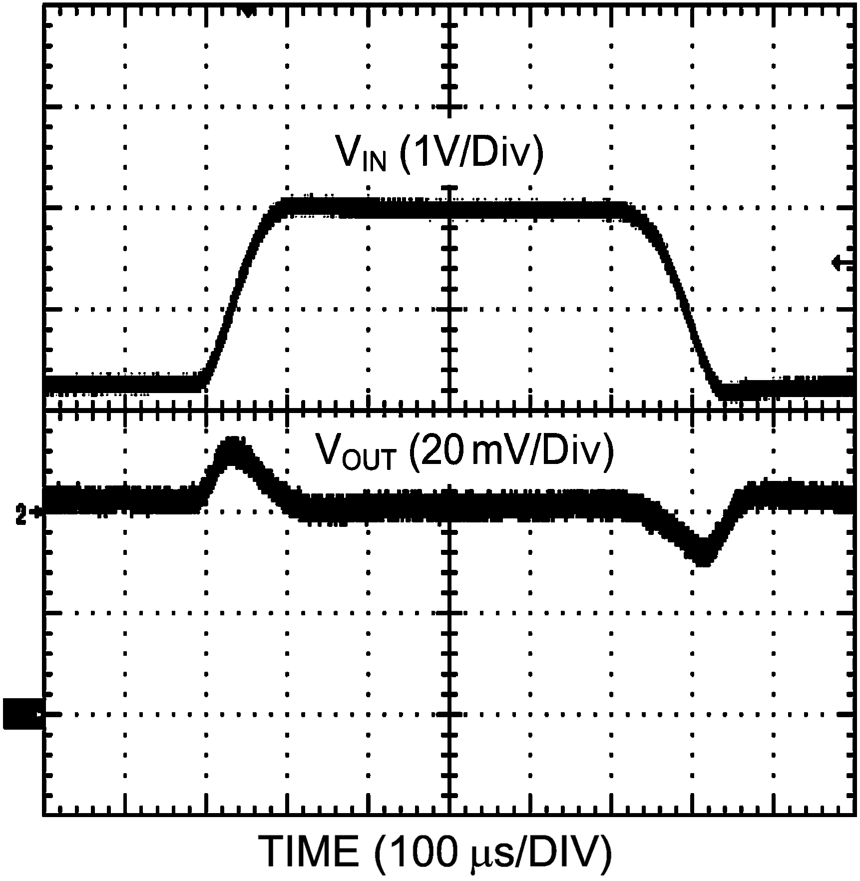 Figure 23. Line Transient Response
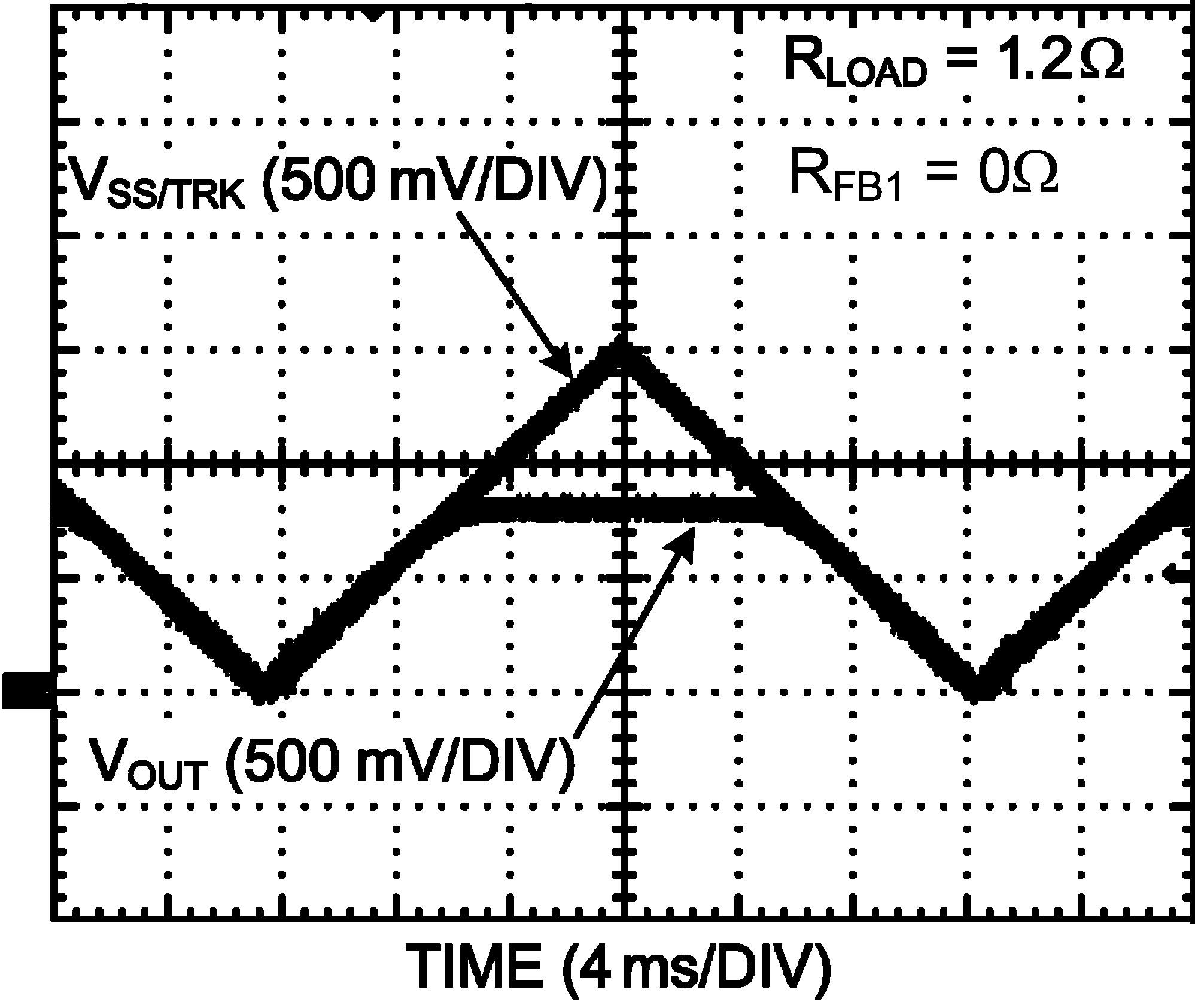 Figure 25. Start Up (Tracking)
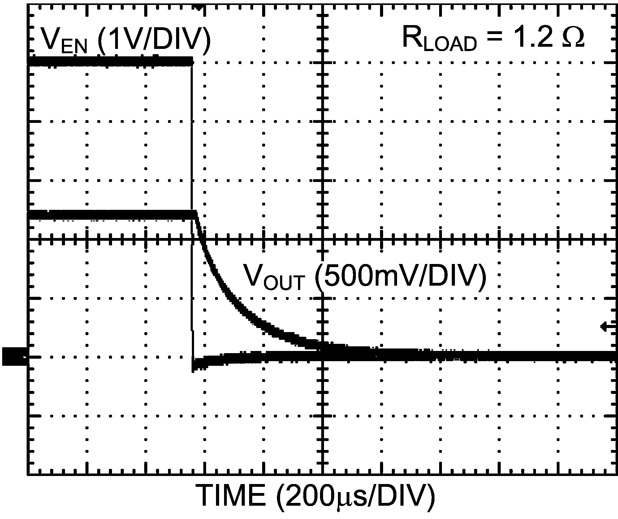 Figure 27. Power Down
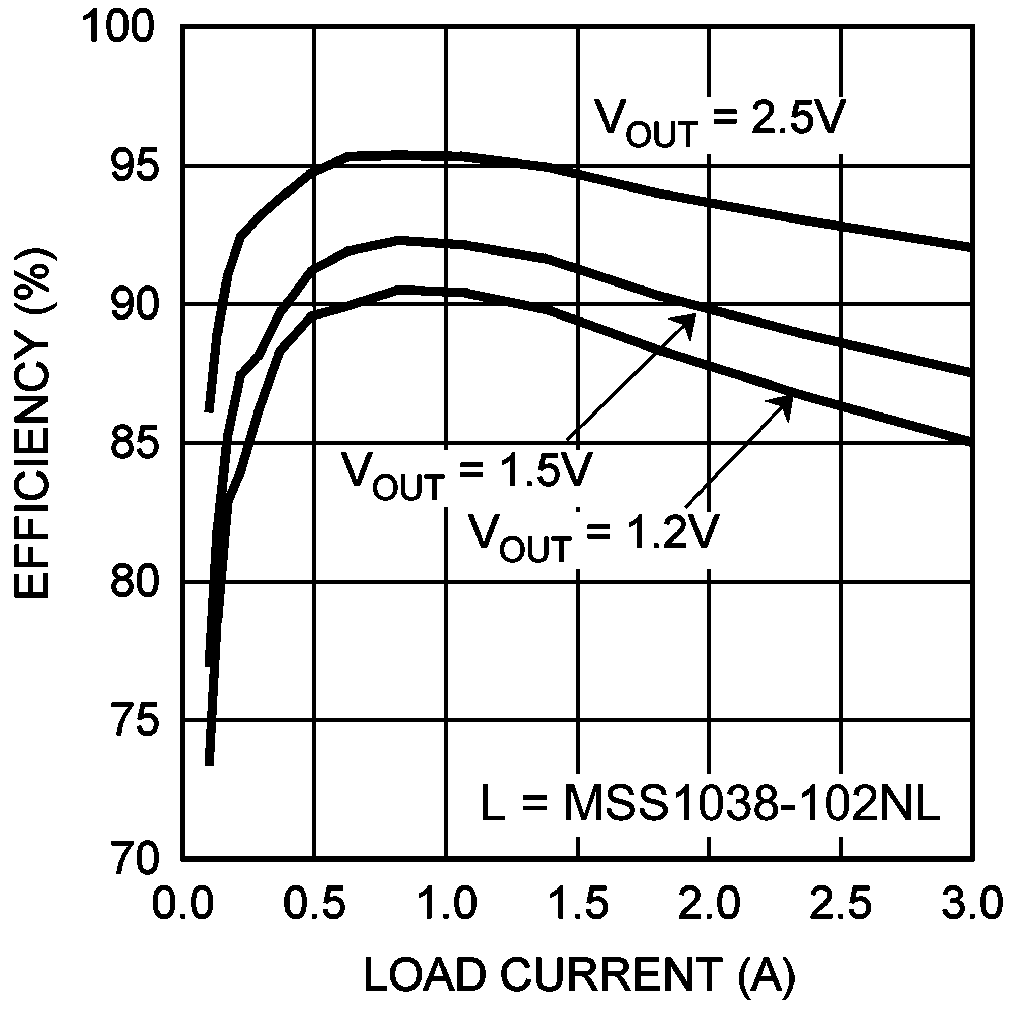
| VIN = 3.3 V | fSW = 1.5 MHz |
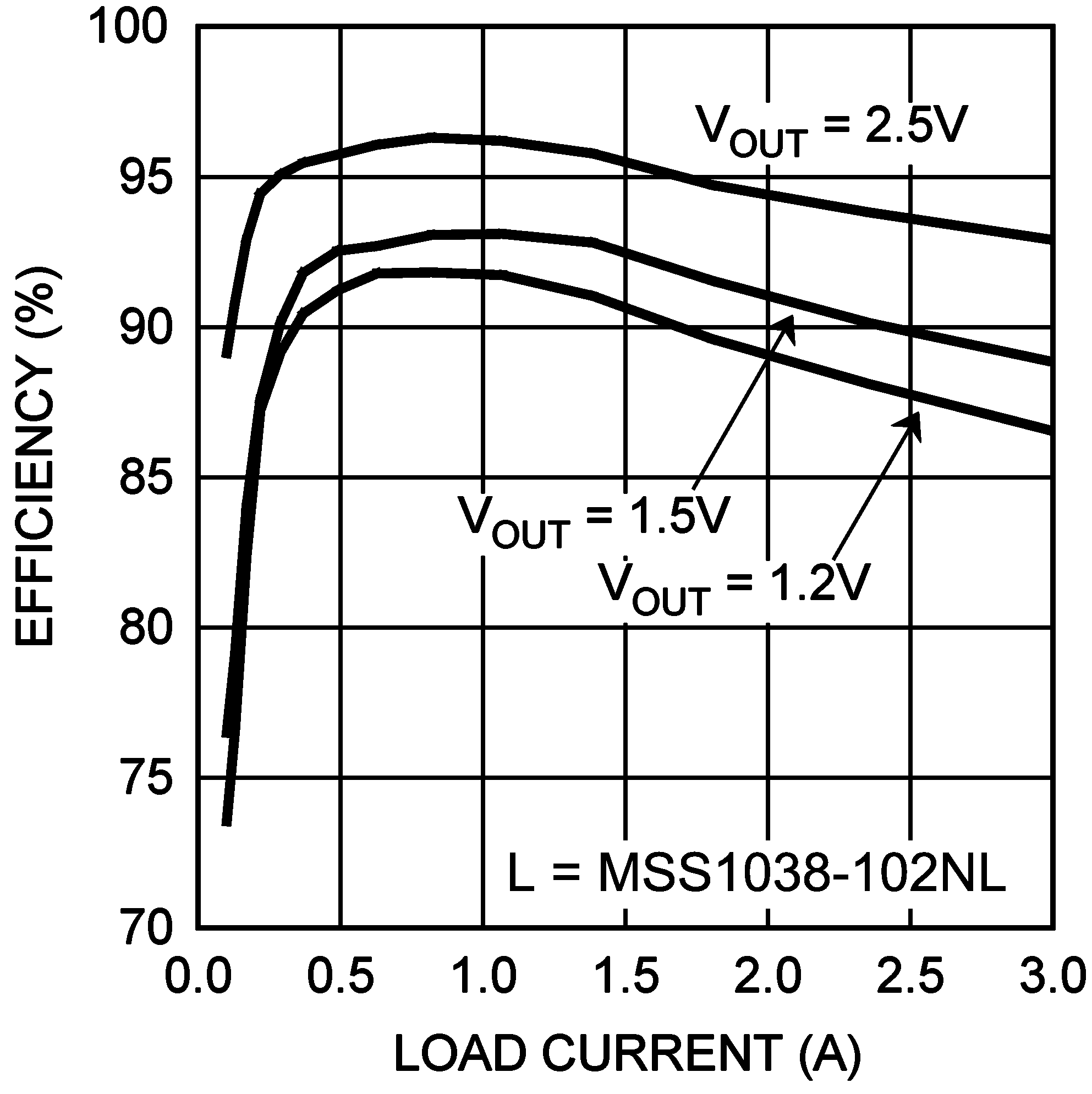
| VIN = 3.3 V | fSW = 1.0 MHz |
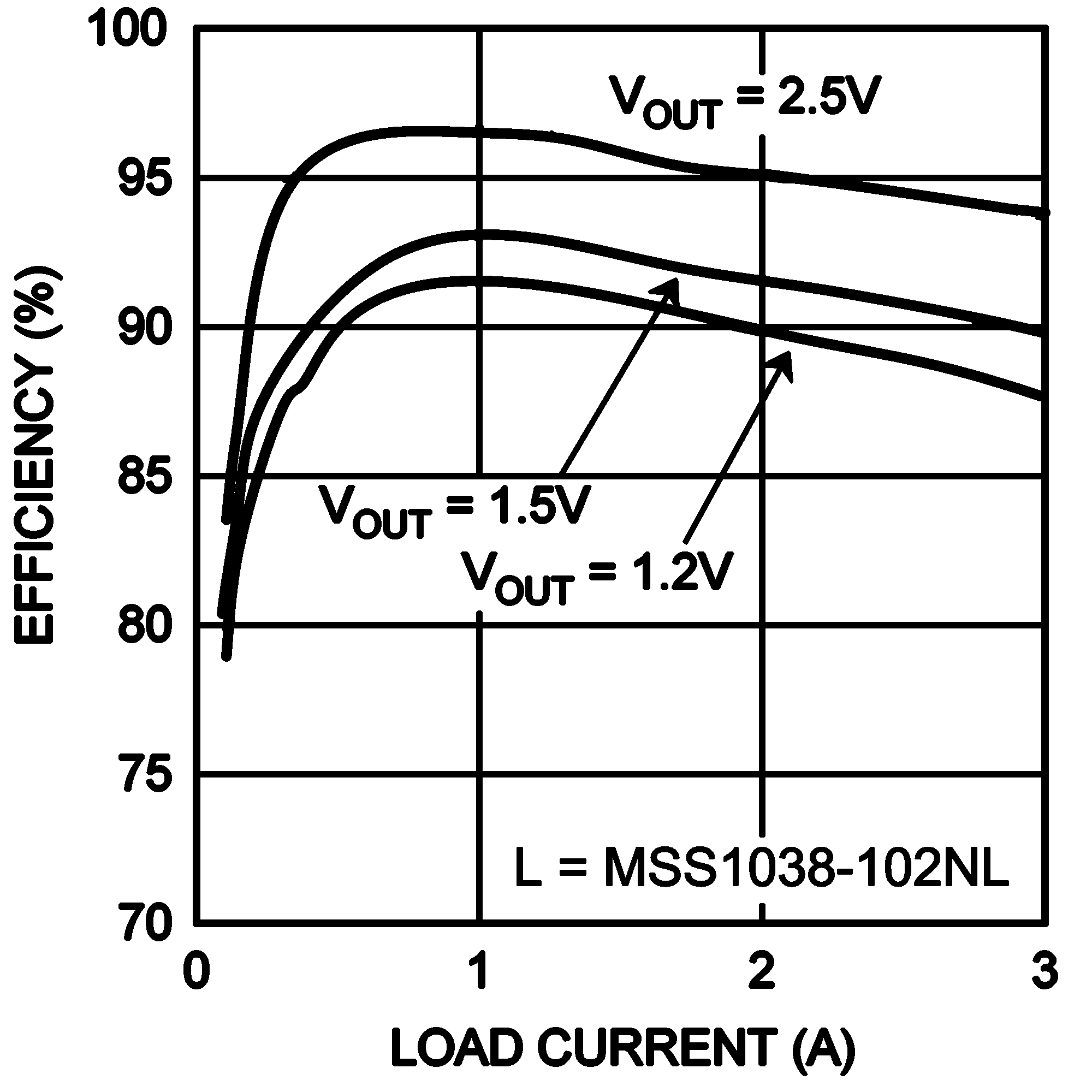
| VIN = 3.3 V | fSW = 500 kHz |
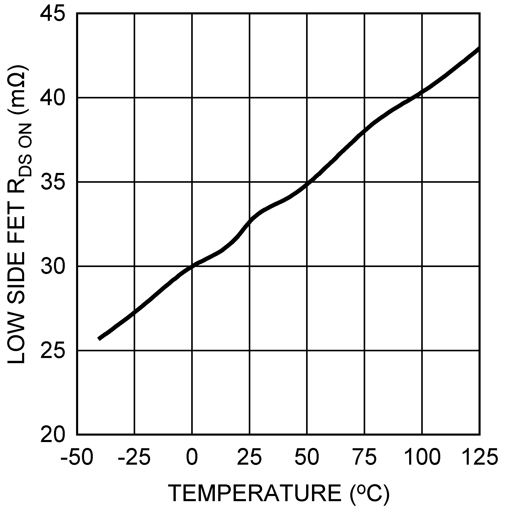 Figure 8. Low-Side FET Resistance vs Temperature
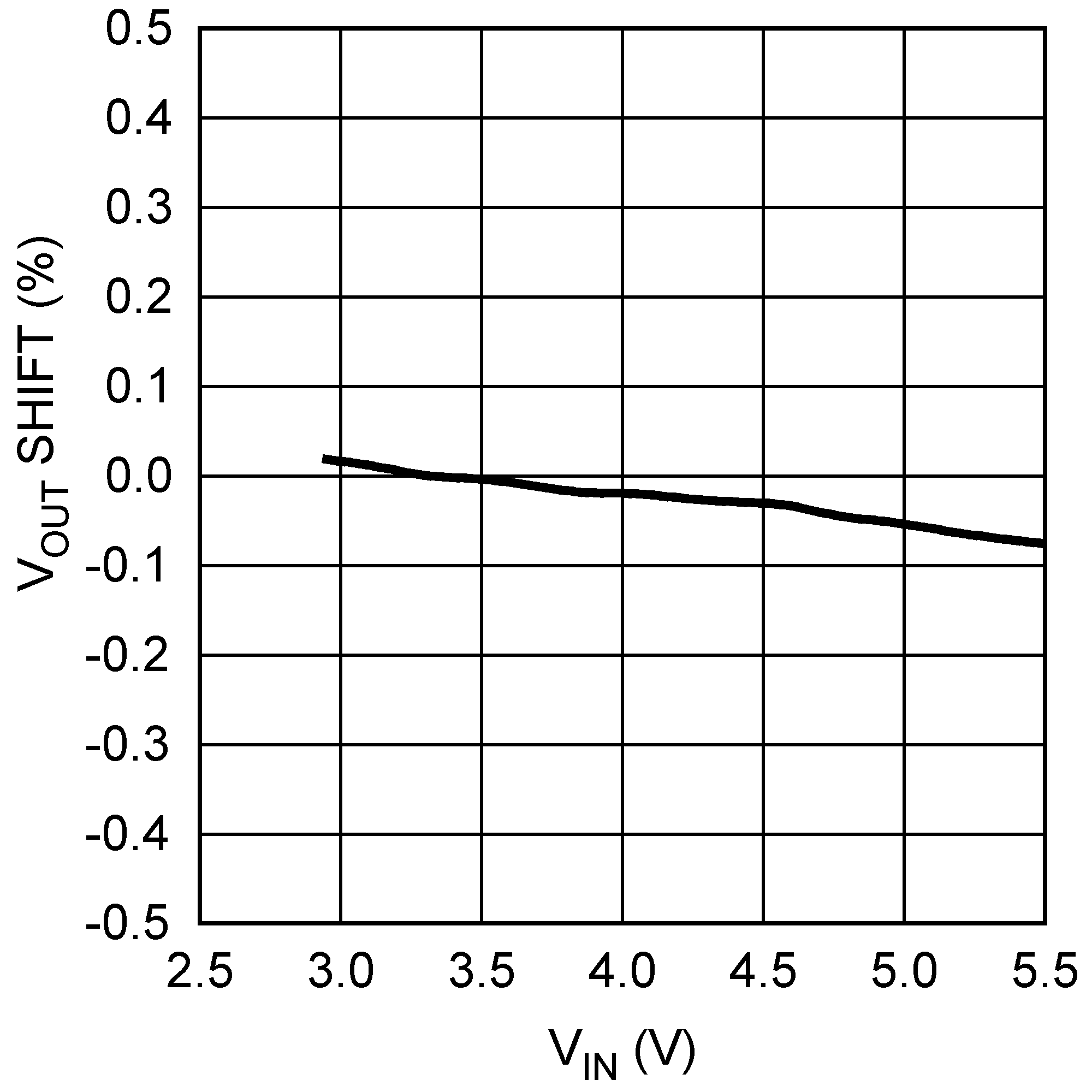 Figure 10. Line Regulation
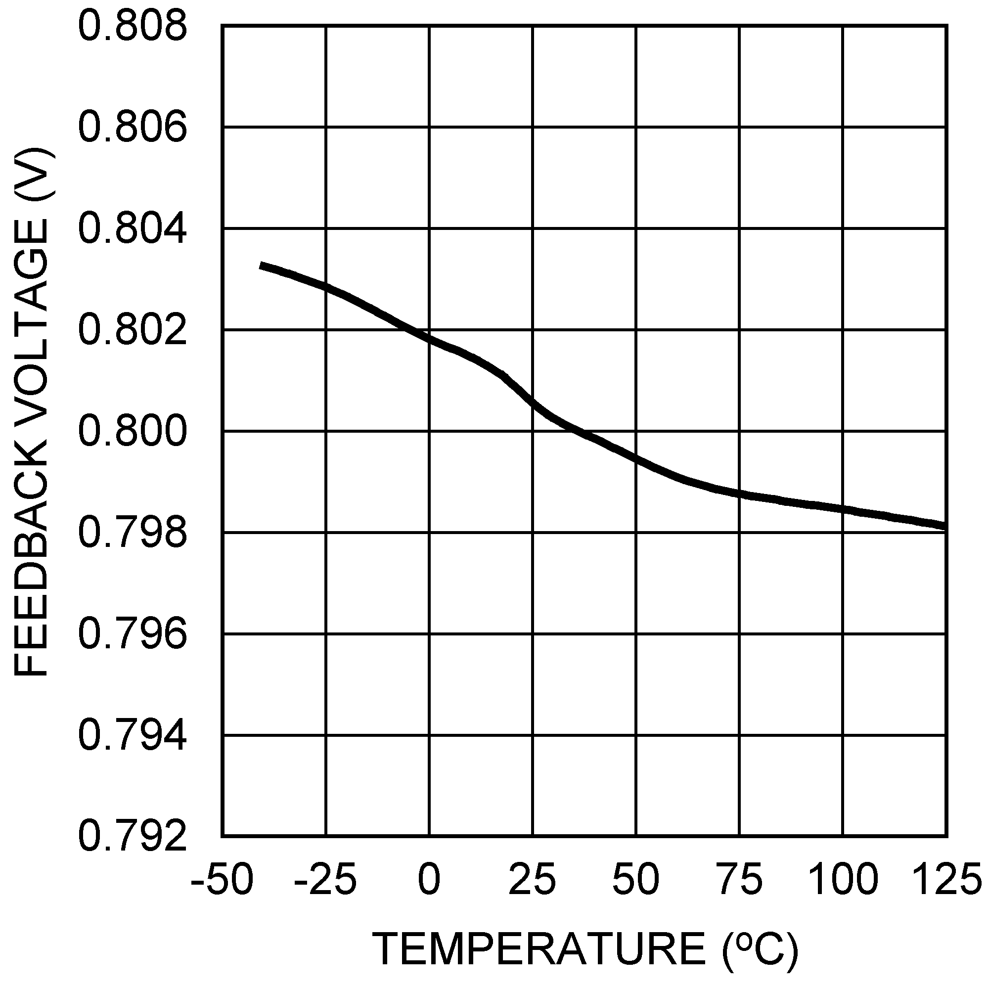 Figure 12. Feedback Pin Voltage vs Temperature
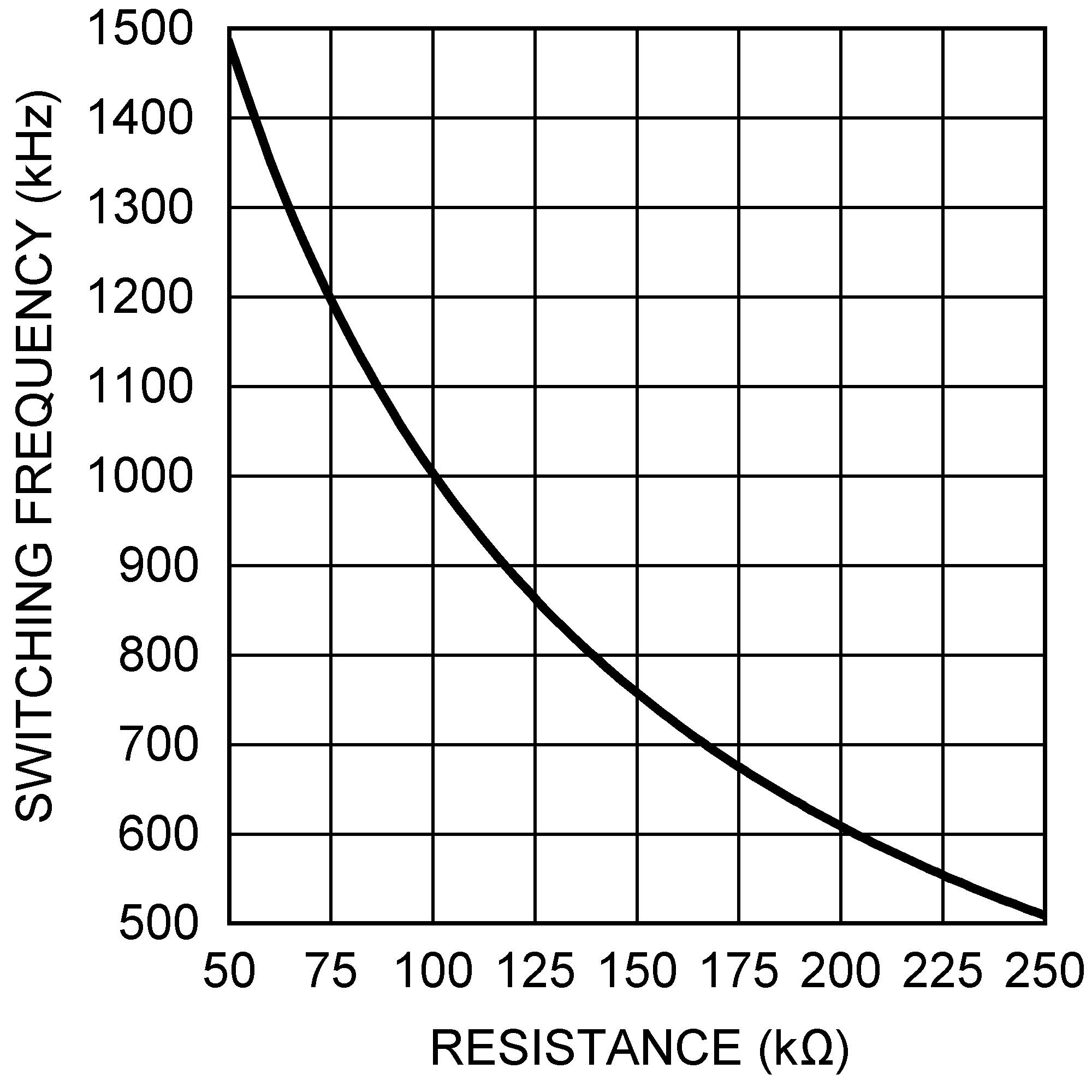 Figure 14. Switching Frequency vs RT
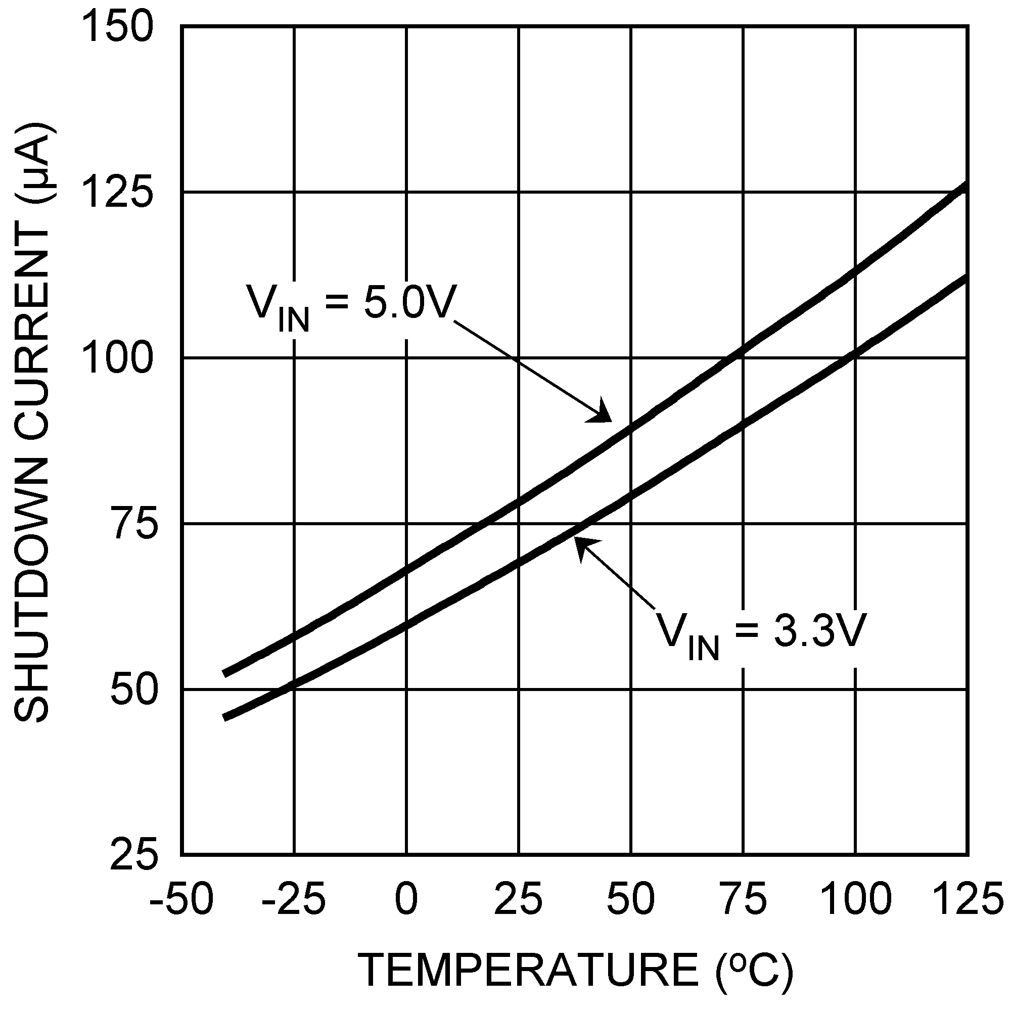 Figure 16. Shutdown Current vs Temperature
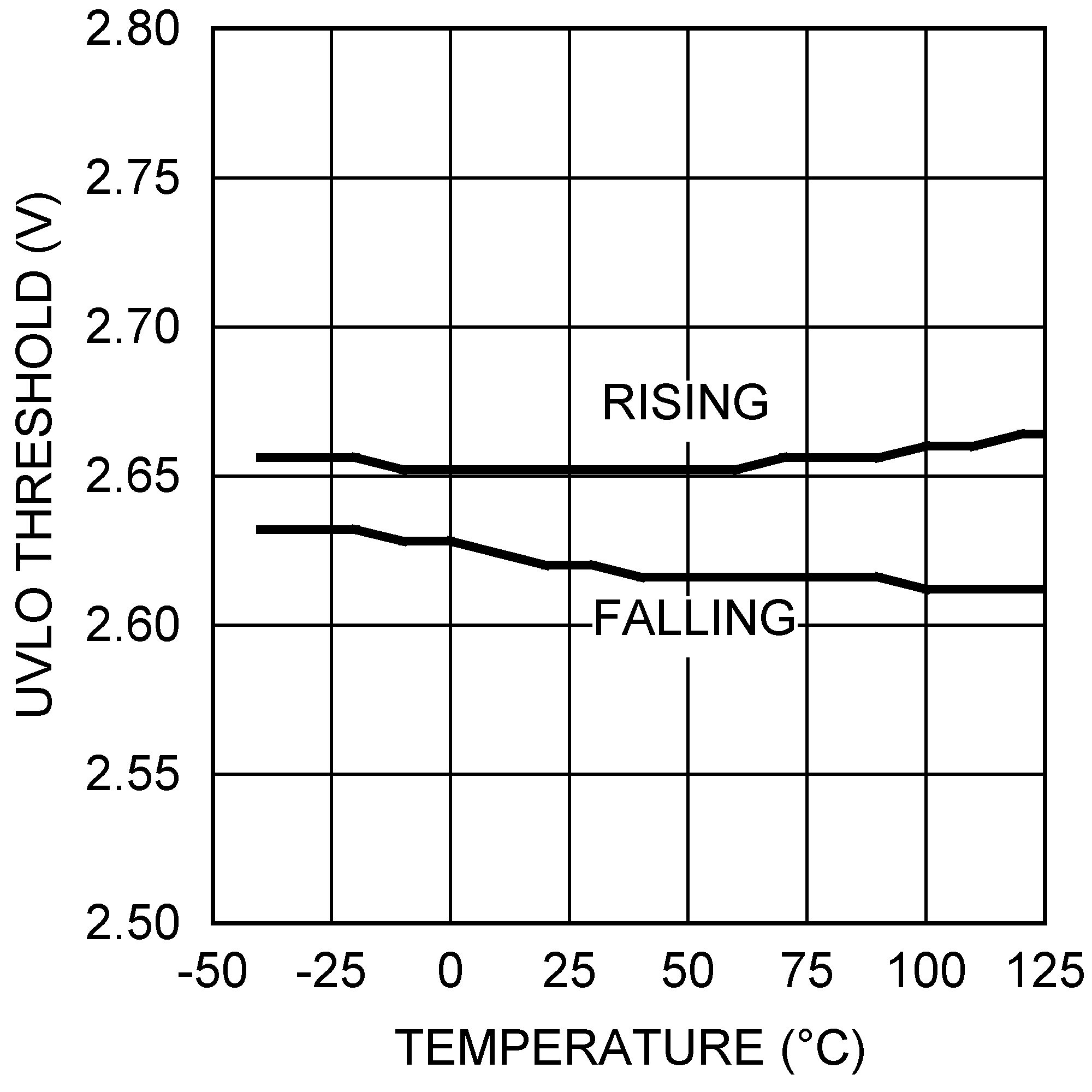 Figure 18. UVLO Threshold vs Temperature
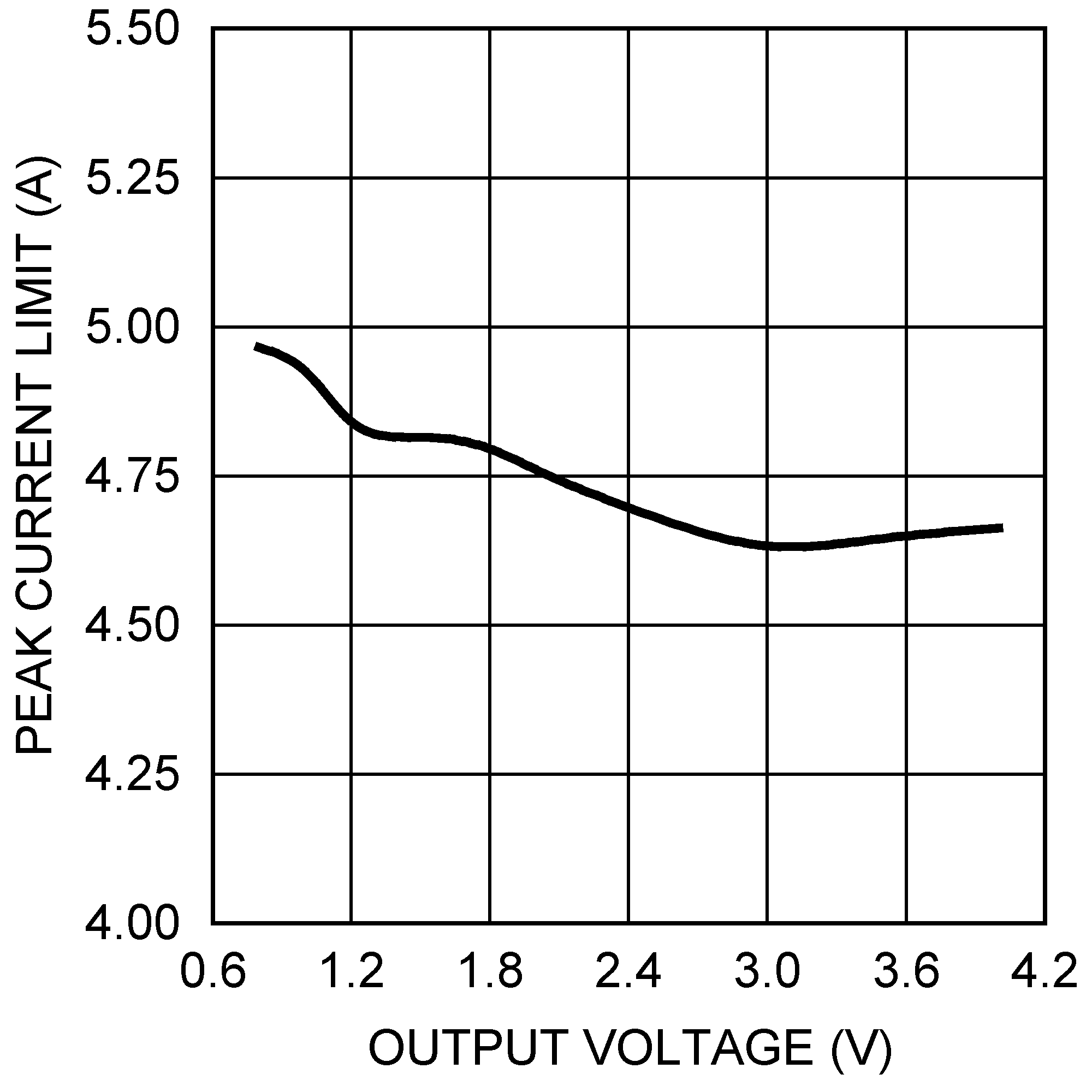 Figure 20. Peak Current Limit vs VOUT
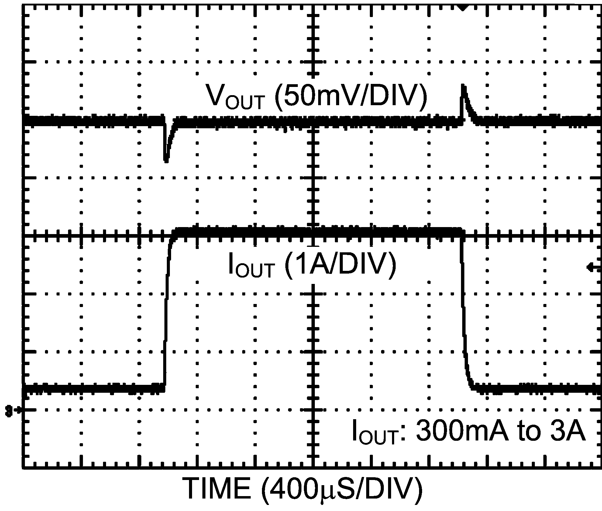 Figure 22. Load Transient Response
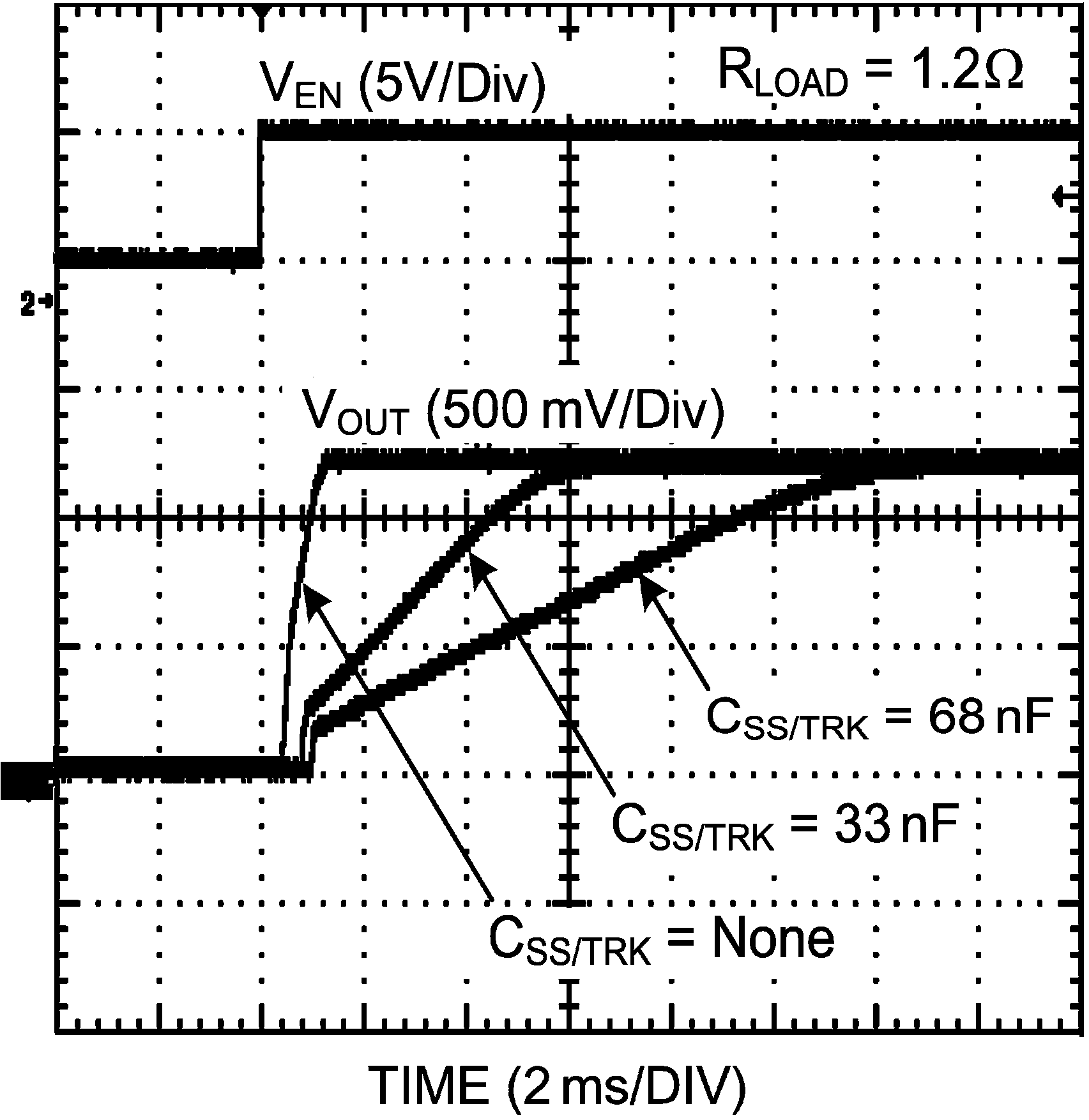 Figure 24. Start Up (Soft-Start)
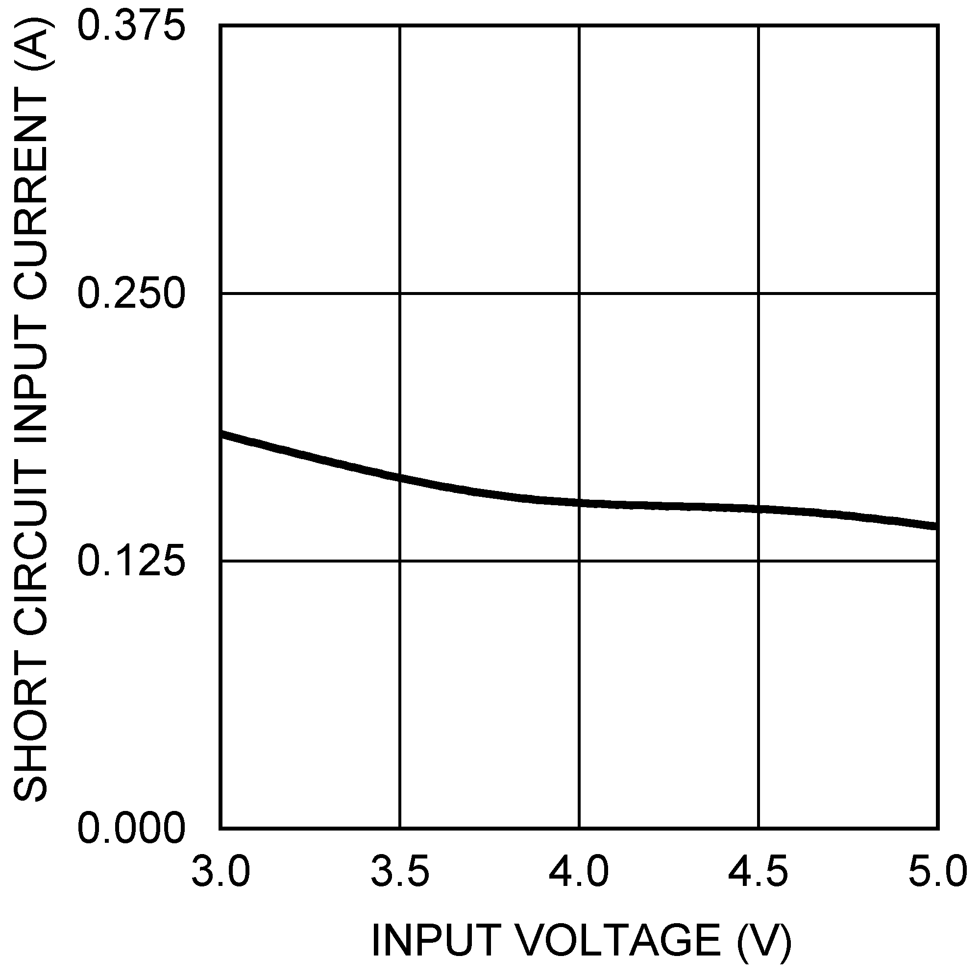 Figure 26. Short Circuit Input Current vs VIN