JAJSBH5B March   2011  – June 2019 LM21212-2

PRODUCTION DATA.  

  1. 特長
  2. アプリケーション
  3. 概要
    1.     Device Images
      1.      アプリケーションの簡略回路図
  4. 改訂履歴
  5. 概要(続き)
  6. Pin Configuration and Functions
    1.     Pin Descriptions
  7. Specifications
    1. 7.1 Absolute Maximum Ratings
    2. 7.2 ESD Ratings
    3. 7.3 Recommended Operating Ratings
    4. 7.4 Electrical Characteristics
    5. 7.5 Typical Characteristics
  8. Detailed Description
    1. 8.1 Overview
    2. 8.2 Functional Block Diagram
    3. 8.3 Feature Description
      1. 8.3.1 Precision Enable
      2. 8.3.2 UVLO
      3. 8.3.3 Current Limit
      4. 8.3.4 Short-Circuit Protection
      5. 8.3.5 Thermal Protection
      6. 8.3.6 Power-Good Flag
      7. 8.3.7 Light Load Operation
    4. 8.4 Device Functional Modes
  9. Application and Implementation
    1. 9.1 Application Information
    2. 9.2 Typical Application
      1. 9.2.1 Typical Application 1
        1. 9.2.1.1 Design Requirements
        2. 9.2.1.2 Detailed Design Procedure
          1. 9.2.1.2.1 Custom Design With WEBENCH® Tools
          2. 9.2.1.2.2 Output Voltage
          3. 9.2.1.2.3 Precision Enable
          4. 9.2.1.2.4 Soft Start
          5. 9.2.1.2.5 Resistor-Adjustable Frequency
          6. 9.2.1.2.6 Inductor Selection
          7. 9.2.1.2.7 Output Capacitor Selection
          8. 9.2.1.2.8 Input Capacitor Selection
          9. 9.2.1.2.9 Control Loop Compensation
        3. 9.2.1.3 Application Curves
      2. 9.2.2 Typical Application Schematic 2
        1. 9.2.2.1 Design Requirements
        2. 9.2.2.2 Detailed Design Procedure
  10. 10Layout
    1. 10.1 Layout Considerations
    2. 10.2 Layout Example
    3. 10.3 Thermal Considerations
  11. 11デバイスおよびドキュメントのサポート
    1. 11.1 デバイス・サポート
      1. 11.1.1 デベロッパー・ネットワークの製品に関する免責事項
      2. 11.1.2 開発サポート
        1. 11.1.2.1 WEBENCH®ツールによるカスタム設計
    2. 11.2 ドキュメントの更新通知を受け取る方法
    3. 11.3 コミュニティ・リソース
    4. 11.4 商標
    5. 11.5 静電気放電に関する注意事項
    6. 11.6 Glossary
  12. 12メカニカル、パッケージ、および注文情報

パッケージ・オプション

メカニカル・データ(パッケージ|ピン)
サーマルパッド・メカニカル・データ
発注情報

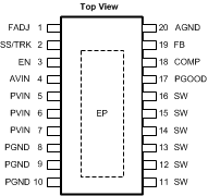
Pin Configuration and Functions

PWP Package
20-Pin HTSSOP Package
Top View
LM21212-2 30155102.gif

Pin Descriptions

PIN
NO. NAME Description
1 FADJ Frequency Adjust pin. The switching frequency can be set to a predetermined rate by connecting a resistor between FADJ and AGND.
2 SS/TRK Soft-start control pin. An internal 2 µA current source charges an external capacitor connected between this pin and AGND to set the output voltage ramp rate during startup. This pin can also be used to configure the tracking feature.
3 EN Active high enable input for the device. If not used, the EN pin can be left open, which will go high due to an internal current source.
4 AVIN Analog input voltage supply that generates the internal bias. It is recommended to connect PVIN to AVIN through a low pass RC filter to minimize the influence of input rail ripple and noise on the analog control circuitry.
5,6,7 PVIN Input voltage to the power switches inside the device. These pins should be connected together at the device. A low ESR input capacitance should be located as close as possible to these pins.
8,9,10 PGND Power ground pins for the internal power switches.
11-16 SW Switch node pins. These pins should be tied together locally and connected to the filter inductor.
17 PGOOD Open-drain power good indicator.
18 COMP Compensation pin is connected to the output of the voltage loop error amplifier.
19 FB Feedback pin is connected to the inverting input of the voltage loop error amplifier.
20 AGND Quiet analog ground for the internal reference and bias circuitry.
EP Exposed Pad Exposed metal pad on the underside of the package with an electrical and thermal connection to PGND. It is recommended to connect this pad to the PC board ground plane in order to improve thermal dissipation.