SNVS639G December 2009 – December 2015 LM21305
PRODUCTION DATA.
- 1 Features
- 2 Applications
- 3 Description
- 4 Revision History
- 5 Description (continued)
- 6 Pin Configuration and Functions
- 7 Specifications
-
8 Detailed Description
- 8.1 Overview
- 8.2 Functional Block Diagram
- 8.3
Feature Description
- 8.3.1 Synchronous DC-DC Switching Converter
- 8.3.2 Peak Current-Mode Control
- 8.3.3 Switching Frequency Setting and Synchronization
- 8.3.4 Light-Load Operation
- 8.3.5 Precision Enable
- 8.3.6 Device Enable, Soft-Start, and Pre-Bias Startup Capability
- 8.3.7 Peak Current Protection and Negative Current Limiting
- 8.3.8 PGOOD Indicator
- 8.3.9 Internal Bias Regulators
- 8.3.10 Minimum On-Time Considerations
- 8.4 Device Functional Modes
-
9 Application and Implementation
- 9.1 Application Information
- 9.2
Typical Application
- 9.2.1 Design Requirements
- 9.2.2
Detailed Design Procedure
- 9.2.2.1 Setting the Output Voltage
- 9.2.2.2 Calculating the Duty Cycle
- 9.2.2.3 Input Capacitors
- 9.2.2.4 AVIN Filter
- 9.2.2.5 Switching Frequency Selection
- 9.2.2.6 Filter Inductor
- 9.2.2.7 Output Capacitor
- 9.2.2.8 Efficiency Considerations
- 9.2.2.9 Load Current Derating When Duty Cycle Exceeds 50%
- 9.2.2.10 Control Loop Compensation
- 9.2.2.11 Compensation Components Selection
- 9.2.2.12 Plotting the Loop Gain
- 9.2.2.13 High Frequency Considerations
- 9.2.2.14 Bootstrap Capacitor
- 9.2.2.15 5V0 and 2V5 Capacitors
- 9.2.2.16 Maximum Ambient Temperature
- 9.2.3 Application Curves
- 10Power Supply Recommendations
- 11Layout
- 12Device and Documentation Support
- 13Mechanical, Packaging, and Orderable Information
7 Specifications
7.1 Absolute Maximum Ratings
see (1)(2)| MIN | MAX | UNIT | |
|---|---|---|---|
| PVIN, AVIN, SW, EN, PGOOD to AGND | −0.3 | 20 | V |
| CBOOT to AGND | −0.3 | 25 | V |
| CBOOT to SW | −0.3 | 5.5 | V |
| 5V0, FB, COMP, FREQ to AGND | −0.3 | 6 | V |
| 2V5 to AGND | −0.3 | 3 | V |
| AGND to PGND | −0.3 | 0.3 | V |
| Maximum continuous power dissipation, PD-MAX(3) | Internally limited | ||
| Junction temperature, TJ-MAX | 150 | °C | |
| Storage temperature, Tstg | –65 | 150 | °C |
(1) Stresses beyond those listed under absolute maximum ratings may cause permanent damage to the device. These are stress ratings only, and functional operation of the device at these or any other conditions beyond those indicated under recommended operating conditions is not implied. Exposure to absolute-maximum-rated conditions for extended periods may affect device reliability.
(2) If Military or Aerospace specified devices are required, please contact the Texas Instruments Sales Office/Distributors for availability and specifications.
(3) The amount of absolute maximum power dissipation allowed in the device depends on the ambient temperature and can be calculated using the formula P = (TJ – TA) / θJA, where TJ is the junction temperature, TA is the ambient temperature, and θJA is the junction-to-ambient thermal resistance. Junction-to-ambient thermal resistance is highly application and board-layout dependent. In applications where high power dissipation exists, special care must be paid to thermal dissipation issues in PCB design. Internal thermal shutdown circuitry protects the device from permanent damage.
(4) In applications where high power dissipation or poor package thermal resistance is present, the maximum ambient temperature may have to be derated. Maximum ambient temperature (TA-MAX) is dependent on the maximum operating junction temperature (TJ-MAX-OP = 125°C), the maximum power dissipation of the device in the application (PD-MAX), and the junction-to ambient thermal resistance of the part or package in the application (θJA), as given by the following equation: TA-MAX = TJ-MAX-OP – (θJA × PD-MAX).
7.2 ESD Ratings
| VALUE | UNIT | |||
|---|---|---|---|---|
| V(ESD) | Electrostatic discharge | Human body model (HBM), per ANSI/ESDA/JEDEC JS-001(1)(3) | ±2000 | V |
| Charged device model (CDM), per JEDEC specification JESD22-C101(2) | ±500 | |||
(1) JEDEC document JEP155 states that 500-V HBM allows safe manufacturing with a standard ESD control process. Manufacturing with less than 500-V HBM is possible with the necessary precautions. Pins listed as ±2000 V may actually have higher performance.
(2) JEDEC document JEP157 states that 250-V CDM allows safe manufacturing with a standard ESD control process. Manufacturing with less than 250-V CDM is possible with the necessary precautions. Pins listed as ±500 V may actually have higher performance.
(3) The human body model is a 100-pF capacitor discharged through a 1.5-kΩ resistor into each pin (MIL-STD-883 3015.7).
7.3 Recommended Operating Conditions
| MIN | MAX | UNIT | |
|---|---|---|---|
| PVIN to PGND, AGND | 3 | 18 | V |
| AVIN to PGND, AGND | 3 | 18 | V |
| Junction temperature | −40 | 125 | °C |
| Ambient temperature(4) | –40 | 85 | °C |
7.4 Thermal Information
| THERMAL METRIC(1) | LM21305 | UNIT | |
|---|---|---|---|
| RSG (WQFN) | |||
| 28 PINS | |||
| RθJA | Junction-to-ambient thermal resistance | 36.9 | °C/W |
| RθJC(top) | Junction-to-case (top) thermal resistance | 22 | °C/W |
| RθJB | Junction-to-board thermal resistance | 9.9 | °C/W |
| ψJT | Junction-to-top characterization parameter | 0.2 | °C/W |
| ψJB | Junction-to-board characterization parameter | 9.8 | °C/W |
| RθJC(bot) | Junction-to-case (bottom) thermal resistance | 2.1 | °C/W |
(1) For more information about traditional and new thermal metrics, see the Semiconductor and IC Package Thermal Metrics application report, SPRA953.
7.5 Electrical Characteristics
All typical limits apply for TJ = 25°C, and all maximum and minimum limits apply over the full operating temperature range (TJ = –40°C to +125°C). Unless otherwise specified, VIN = VPVIN = VAVIN = 12 V, VOUT = 3.3 V, IOUT = 0 A.(1)(2)(2)| PARAMETER | TEST CONDITIONS | MIN | TYP | MAX | UNIT | |
|---|---|---|---|---|---|---|
| GENERAL | ||||||
| VFB-default | Feedback pin factory-default voltage | 0.588 | 0.598 | 0.608 | V | |
| ΔVOUT/ΔIOUT | Load regulation | IOUT = 0.1 A to 5 A | 0.02 | %/A | ||
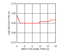
| ΔVOUT/ΔVIN | Line regulation | VPVIN = 3 V to 18 V | 0.01 | %/V | ||
| RDSonHS | High-side switch on-resistance | IDS = 5 A | 44 | mΩ | ||
| RDSonLS | Low-side switch on-resistance | IDS = 5 A | 22 | mΩ | ||
| ICL-HS | High-side switch current limit | High-side MOSFET | 5.9 | 7 | 7.87 | A |
| ICL-LS | Low-side switch current limit | Low-side MOSFET(3) | 5.9 | 8 | 10.2 | A |
| INEG-CL-LS | Low-side switch negative current limit | Low-side MOSFET | –7 | –4.1 | –1.64 | A |
| ISD | Quiescent current, disabled | VAVIN = V PVIN = 5 V | 0.1 | 2 | µA | |
| VAVIN = V PVIN = 18 V | 1 | 4.1 | ||||
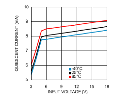
| IQ | Quiescent current, enabled, not switching | VAVIN = V PVIN = 18 V | 9 | 9.7 | mA | |
| IFB | Feedback pin input bias current | VFB = 0.598 V | 1 | nA | ||
| GM | Error amplifier transconductance | 2400 | µs | |||
| AVOL | Error amplifier voltage gain | 65 | dB | |||
| VIH-OVP | OVP tripping threshold | Rising threshold, percentage of VOUT | 103.5% | 109.5% | 115% | |
| VHYST-OVP | OVP hysteresis window | Percentage of VOUT | –4.3% | |||
| VUVLO-HI-AVIN | AVIN UVLO rising threshold | 2.84 | 2.93 | 2.987 | V | |
| VUVLO-LO-AVIN | AVIN UVLO falling threshold | 2.66 | 2.73 | 2.83 | V | |
| VUVLO-HYS-AVIN | AVIN UVLO hysteresis window | 195 | mV | |||
| V5V0 | Internal LDO1 output voltage | Measured at 5V0 pin, 1-kΩ load | 4.88 | V | ||
| COUT-CAP-5V0 | Recommended capacitance connected to 5V0 pin | Ceramic capacitor | 1 | µF | ||
| GENERAL (continued) | ||||||
| ISHORT-5V0 | Short-circuit current of 5V0 pin | 31 | mA | |||
| V2V5 | Internal LDO2 output voltage | Measured at 2V5 pin, 1-kΩ load | 2.47 | V | ||
| COUT-CAP-2V5 | Recommended capacitance connected to 2V5 pin | Ceramic capacitor | 100 | nF | ||
| ISHORT-2V5 | Short-circuit current of 2V5 pin | 47 | mA | |||
| VFCBOOT-D | CBOOT diode forward voltage | Measured from 5V0 to CBOOT at 10 mA | 0.76 | V | ||
| ICBOOT | CBOOT leakage current | VCBOOT = 5.5 V, not switching | 0.65 | µA | ||
| TSTARTUP-DELAY | Startup time from EN high to the beginning of internal soft-start | 160 | µs | |||
| SS | Internal soft-start | 10% to 90% VFB | 1.41 | 2.7 | 4.15 | ms |
| OSCILLATOR | ||||||
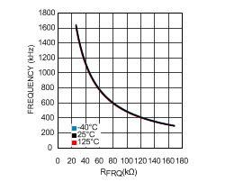
| FOSC-NOM | Oscillator frequency, nominal measured at SW pin | RFRQ = 61.9 kΩ, 0.025% | 695 | 750 | 795 | kHz |
| FOSC-MAX | Maximum oscillator frequency measured at SW pin | RFRQ = 28.4 kΩ | 1500 | kHz | ||
| FOSC-MIN | Minimum oscillator frequency measured at SW pin | RFRQ = 167.5 kΩ | 300 | kHz | ||
| TOFF-MIN | Minimum off-time measured at SW pin | FSW = 1.5 MHz, VIN = 3.3 V, VFB = 1 V, voltage divider ratio = 3.3 | 50 | ns | ||
| TON-MIN | Minimum on-time measured at SW pin | FSW = 1.5 MHz, voltage divider ratio = 1 | 70 | ns | ||
| LOGIC | ||||||
| VIH-EN | EN pin rising threshold | 1.1 | 1.2 | 1.3 | V | |
| VHYST-EN | EN pin hysteresis window | 130 | 200 | 302 | mV | |
| IEN-IN | EN pin input current | VEN = 12 V | 18 | 23 | µA | |
| VIH-UV-PGOOD | PGOOD UV rising threshold | Percentage of VOUT | 87.5% | 93% | 97.5% | |
| VHYST-UV-PGOOD | PGOOD UV hysteresis threshold | Percentage of VOUT | –4.2% | |||
| IOL- PGOOD | PGOOD sink current | VOL = 0.2 V | 3 | mA | ||
| IOH- PGOOD | PGOOD leakage current | VOH = 18 V | 460 | nA | ||
| THERMAL SHUTDOWN | ||||||
| TSD | Thermal shutdown(4) | 160 | °C | |||
| TSD-HYS | Thermal shutdown hysteresis(4) | 10 | °C | |||
(1) All limits are specified by design, test or statistical analysis. All electrical characteristics having room-temperature limits are tested during production with TJ = 25°C. All hot and cold limits are specified by correlating the electrical characteristics to process and temperature variations and applying statistical process control.
(2) Capacitors: low ESR surface-mount ceramic capacitors (MLCCs) are used in setting electrical characteristics.
(3) The low-side switch current limit is ensured to be higher than the high-side current limit.
(4) Specified by design.
7.6 Typical Characteristics
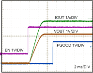
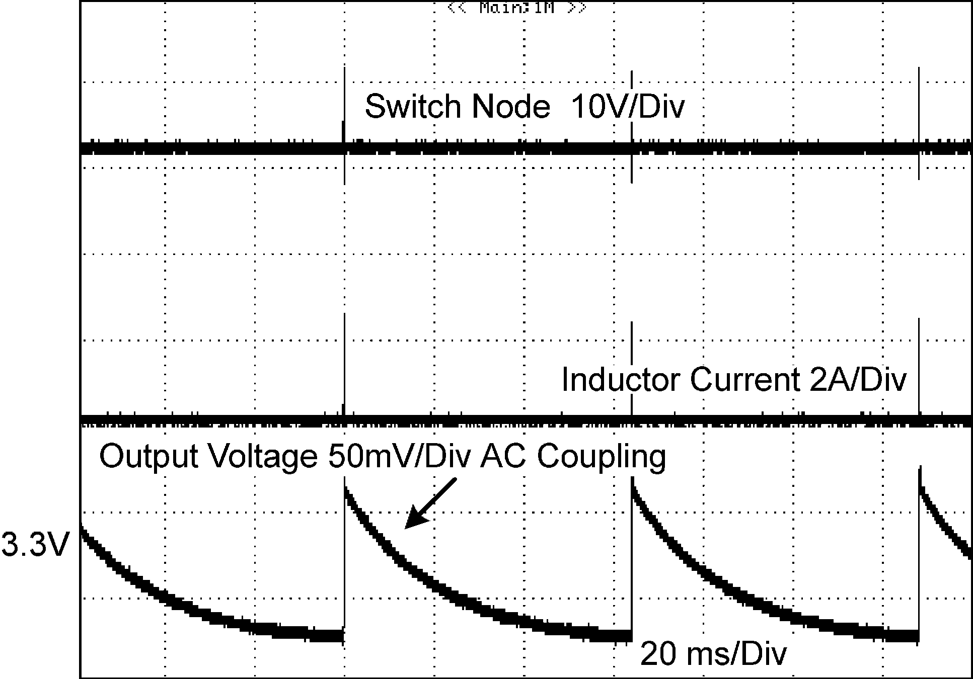
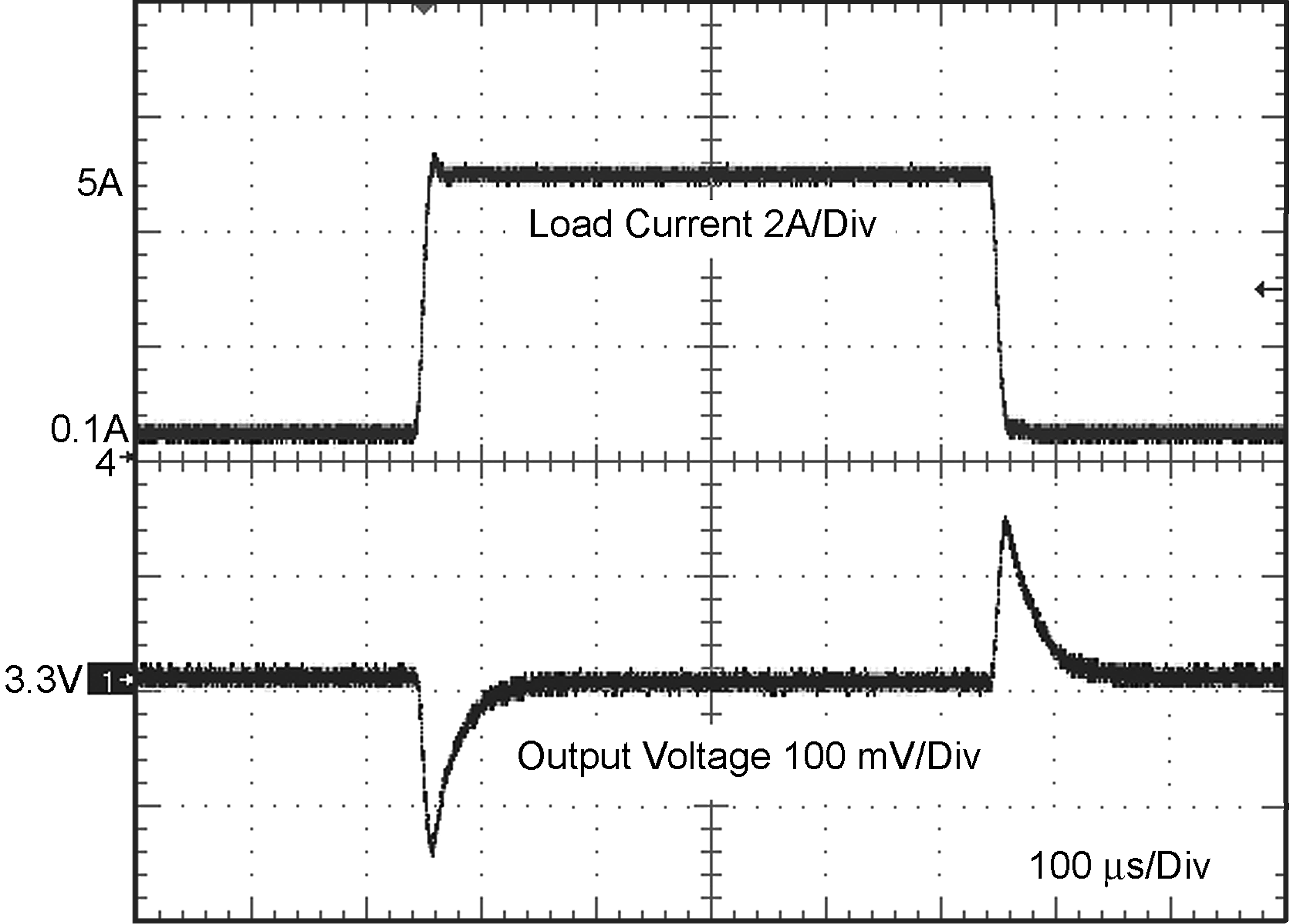
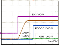
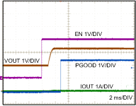
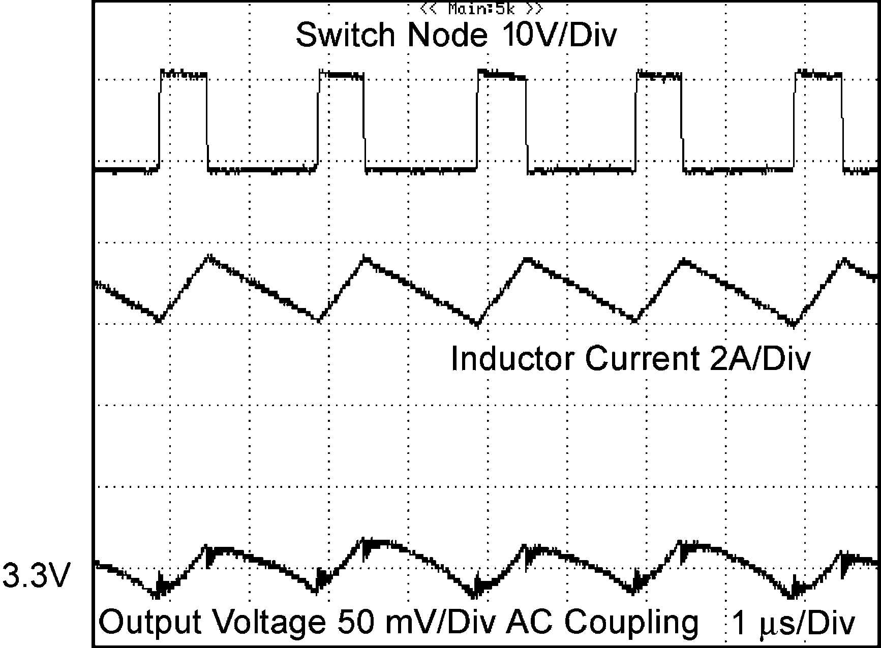
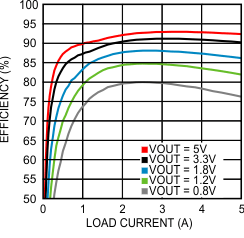
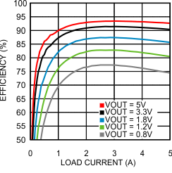
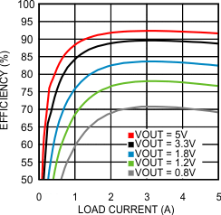
VIN = 12 V, VOUT = 3.3 V, FSW = 500 kHz, TA = 25°C, L = 3.3 µH, and COUT = 100 µF (ceramic), (unless otherwise specified)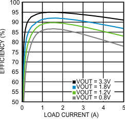
| FSW = 300 kHz |
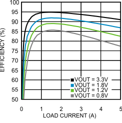
| FSW = 500 kHz |
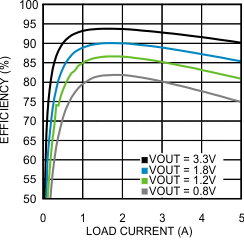
| FSW = 1 MHz |
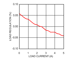
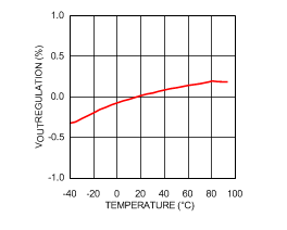
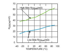
vs Temperature
| FSW = 300 kHz |
| FSW = 500 kHz |
| FSW = 1 MHz |
