JAJSBQ6X October 1979 – October 2023 LM139 , LM139A , LM239 , LM239A , LM2901 , LM2901AV , LM2901B , LM2901V , LM339 , LM339A , LM339B
PRODMIX
- 1
- 1 特長
- 2 アプリケーション
- 3 概要
- 4 Revision History
- 5 Other Versions
- 6 Pin Configuration and Functions
-
7 Specifications
- 7.1 Absolute Maximum Ratings for LM339B and LM2901B
- 7.2 Absolute Maximum Ratings for Non-B Versions
- 7.3 ESD Ratings for LM339B and LM2901B
- 7.4 ESD Ratings, Non-B Versions
- 7.5 Recommended Operating Conditions for LM339B and LM2901B
- 7.6 Recommended Operating Conditions, Non-B Versions
- 7.7 Thermal Information for LM339B and LM2901B
- 7.8 Thermal Information for Non-B Versions
- 7.9 Electrical Characteristics for LM339B
- 7.10 Electrical Characteristics for LM2901B
- 7.11 Electrical Characteristics for LM139 and LM139A
- 7.12 Electrical Characteristics for LMx39 and LMx39A
- 7.13 Electrical Characteristics for LM2901, LM2901V and LM2901AV
- 7.14 Switching Characteristics for LM139 and LM139A
- 7.15 Switching Characteristics for LM339B and LM2901B
- 7.16 Switching Characteristics for LMx39 and LMx39A
- 7.17 Switching Characteristics for LM2901
- 7.18 Typical Characteristics for LM339B and LM2901B Only
- 7.19 Typical Characteristics, Non-B Versions
- 8 Detailed Description
- 9 Application and Implementation
- 10Device and Documentation Support
- 11Mechanical, Packaging, and Orderable Information
パッケージ・オプション
デバイスごとのパッケージ図は、PDF版データシートをご参照ください。
メカニカル・データ(パッケージ|ピン)
- D|14
- PW|14
- N|14
サーマルパッド・メカニカル・データ
発注情報
7.19 Typical Characteristics, Non-B Versions
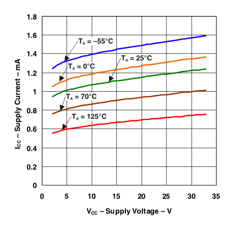 Figure 7-33 Supply Current vs Supply Voltage
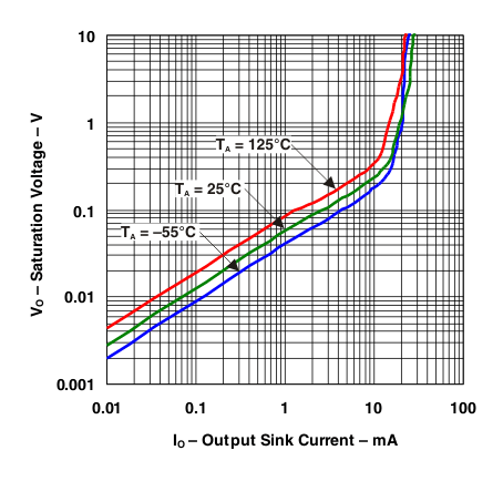 Figure 7-35 Output Saturation Voltage
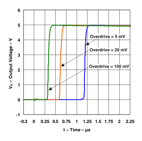 Figure 7-37 Response Time for Various Overdrives Positive Transition
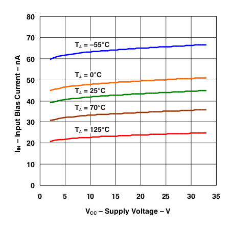 Figure 7-34 Input Bias Current vs Supply Voltage
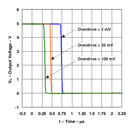 Figure 7-36 Response Time for Various Overdrives Negative Transition