SNVS654J February 2010 – December 2015 LM25066
PRODUCTION DATA.
- 1 Features
- 2 Applications
- 3 Description
- 4 Revision History
- 5 Description (continued)
- 6 Pin Configuration and Functions
- 7 Specifications
-
8 Detailed Description
- 8.1 Overview
- 8.2 Functional Block Diagram
- 8.3 Feature Description
- 8.4 Device Functional Modes
- 8.5
Register Maps
- 8.5.1
PMBus Command Support
- 8.5.1.1
Standard PMBus™ Commands
- 8.5.1.1.1 OPERATION (01h)
- 8.5.1.1.2 CLEAR_FAULTS (03h)
- 8.5.1.1.3 CAPABILITY (19h)
- 8.5.1.1.4 VOUT_UV_WARN_LIMIT (43h)
- 8.5.1.1.5 OT_FAULT_LIMIT (4Fh)
- 8.5.1.1.6 OT_WARN_LIMIT (51h)
- 8.5.1.1.7 VIN_OV_WARN_LIMIT (57h)
- 8.5.1.1.8 VIN_UV_WARN_LIMIT (58h)
- 8.5.1.1.9 STATUS_BYTE (78h)
- 8.5.1.1.10 STATUS_WORD (79h)
- 8.5.1.1.11 STATUS_VOUT (7Ah)
- 8.5.1.1.12 STATUS_INPUT (7Ch)
- 8.5.1.1.13 STATUS_TEMPERATURE (7Dh)
- 8.5.1.1.14 STATUS_CML (7Eh)
- 8.5.1.1.15 STATUS_MFR_SPECIFIC (80h)
- 8.5.1.1.16 READ_VIN (88h)
- 8.5.1.1.17 READ_VOUT (8Bh)
- 8.5.1.1.18 READ_TEMPERATURE_1 (8Dh)
- 8.5.1.1.19 MFR_ID (99h)
- 8.5.1.1.20 MFR_MODEL (9Ah)
- 8.5.1.1.21 MFR_REVISION (9Bh)
- 8.5.1.2
Manufacturer Specific PMBus™ Commands
- 8.5.1.2.1 MFR_SPECIFIC_00: READ_VAUX (D0h)
- 8.5.1.2.2 MFR_SPECIFIC_01: MFR_READ_IIN (D1h)
- 8.5.1.2.3 MFR_SPECIFIC_02: MFR_READ_PIN (D2h)
- 8.5.1.2.4 MFR_SPECIFIC_03: MFR_IN_OC_WARN_LIMIT (D3h)
- 8.5.1.2.5 MFR_SPECIFIC_04: MFR_PIN_OP_WARN_LIMIT (D4h)
- 8.5.1.2.6 MFR_SPECIFIC_05: READ_PIN_PEAK (D5h)
- 8.5.1.2.7 MFR_SPECIFIC_06: CLEAR_PIN_PEAK (D6h)
- 8.5.1.2.8 MFR_SPECIFIC_07: GATE_MASK (D7h)
- 8.5.1.2.9 MFR_SPECIFIC_08: ALERT_MASK (D8h)
- 8.5.1.2.10 MFR_SPECIFIC_09: DEVICE_SETUP (D9h)
- 8.5.1.2.11 MFR_SPECIFIC_10: BLOCK_READ (DAh)
- 8.5.1.2.12 MFR_SPECIFIC_11: SAMPLES_FOR_AVG (DBh)
- 8.5.1.2.13 MFR_SPECIFIC_12: READ_AVG_VIN (DCh)
- 8.5.1.2.14 MFR_SPECIFIC_13: READ_AVG_VOUT (DDh)
- 8.5.1.2.15 MFR_SPECIFIC_14: READ_AVG_IIN (DEh)
- 8.5.1.2.16 MFR_SPECIFIC_15: READ_AVG_PIN (DFh)
- 8.5.1.2.17 MFR_SPECIFIC_16: BLACK_BOX_READ (E0h)
- 8.5.1.2.18 MFR_SPECIFIC_17: READ_DIAGNOSTIC_WORD (E1h)
- 8.5.1.2.19 MFR_SPECIFIC_18: AVG_BLOCK_READ (E2h)
- 8.5.1.3 Reading and Writing Telemetry Data and Warning Thresholds
- 8.5.1.4 Determining Telemetry Coefficients Empirically With Linear Fit
- 8.5.1.5 Writing Telemetry Data
- 8.5.1.6 PMBus™ Address Lines (ADR0, ADR1, ADR2)
- 8.5.1.7 SMBA Response
- 8.5.1.1
Standard PMBus™ Commands
- 8.5.1
PMBus Command Support
-
9 Application and Implementation
- 9.1 Application Information
- 9.2
Typical Application
- 9.2.1
12-V, 45-A PMBus Hotswap Design
- 9.2.1.1 Design Requirements
- 9.2.1.2
Detailed Design Procedure
- 9.2.1.2.1 Select RSNS and CL Setting
- 9.2.1.2.2 Selecting the Hotswap FETs
- 9.2.1.2.3 Select Power Limit
- 9.2.1.2.4 Set Fault Timer
- 9.2.1.2.5 Check MOSFET SOA
- 9.2.1.2.6 Switching to dV/dt based Start-up
- 9.2.1.2.7 Choosing the VOUT Slew Rate
- 9.2.1.2.8 Select Power Limit and Fault Timer
- 9.2.1.2.9 Set Undervoltage and Overvoltage Threshold
- 9.2.1.2.10 Power Good Pin
- 9.2.1.2.11 Input and Output Protection
- 9.2.1.2.12 Final Schematic and Component Values
- 9.2.2 Application Curves
- 9.2.1
12-V, 45-A PMBus Hotswap Design
- 10Power Supply Recommendations
- 11Layout
- 12Device and Documentation Support
- 13Mechanical, Packaging, and Orderable Information
1 Features
- Input Voltage Range: 2.9 V to 17 V
- I2C/SMBus Interface and PMBus™ Compliant Command Structure
- Programmable 25-mV or 46-mV Current Limit Threshold
- Configurable Circuit Breaker Protection for Hard Shorts
- Configurable Undervoltage and Overvoltage Lockouts With Hysteresis
- Remote Temperature Sensing With Programmable Warning and Shutdown Thresholds
- Detection and Notification of Damaged MOSFET Condition
- Real-Time Monitoring of VIN, VOUT, IIN, PIN, VAUX With 12-bit Resolution and 1-kHz Sampling Rate
- Current Measurement Accuracy: ±2.4% Over Temperature
- Power Measurement Accuracy: ±3% Over Temperature
- True Input Power Measurement Using Simultaneous Sampling of VIN and IIN Accurately Averages Dynamic Power Readings
- Averaging of VIN, IIN, PIN, and VOUT Over Programmable Interval Ranging from 0.001 to
4 Seconds - Programmable WARN and FAULT Thresholds With SMBA Notification
- Blackbox Capture of Telemetry Measurements and Device Status Triggered by WARN or FAULT Condition
- Full-Featured Application Design and Development GUI
- 24-Lead WQFN Package
2 Applications
- Server Backplane Systems
- Basestation Power Distribution Systems
- Solid-State Circuit Breaker
3 Description
The LM25066 combines a high-performance hot-swap controller with a PMBus™ compliant SMBus/I2C interface to accurately measure, protect and control the electrical operating conditions of computing and storage blades connected to a backplane power bus. The LM25066 continuously supplies real-time power, voltage, current, temperature and fault data to the system management host via the SMBus interface.
The LM25066 control block includes a unique hot-swap architecture that provides current and power limiting to protect sensitive circuitry during insertion of boards into a live system backplane, or any other hot power source. A fast acting circuit breaker prevents damage in the event of a short circuit on the output. The input undervoltage and overvoltage levels and hysteresis are configurable, as well as the insertion delay time and fault detection time. A temperature monitoring block on the LM25066 interfaces with a low-cost external diode for monitoring the temperature of the external MOSFET or other thermally sensitive components. The POWER GOOD output provides a fast indicator when the input and/or output voltages are outside their programmed range. LM25066 current measurement accuracy is ±2.4% over temperature.
Device Information(1)
| PART NUMBER | PACKAGE | BODY SIZE (NOM) |
|---|---|---|
| LN25066 | WQFN (24) | 5.00 mm × 4.00 mm |
- For all available packages, see the orderable addendum at the end of the data sheet.
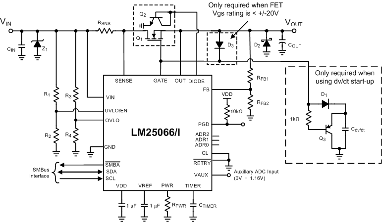
Typical Application Schematic
