JAJSDG8F July 2011 – March 2018 LM25118
PRODUCTION DATA.
- 1 特長
- 2 アプリケーション
- 3 概要
- 4 改訂履歴
- 5 Pin Configuration and Functions
- 6 Specifications
- 7 Detailed Description
-
8 Application and Implementation
- 8.1 Application Information
- 8.2
Typical Application
- 8.2.1 Design Requirements
- 8.2.2
Detailed Design Procedure
- 8.2.2.1 Custom Design With WEBENCH® Tools
- 8.2.2.2 R7 = RT
- 8.2.2.3 Inductor Selection – L1
- 8.2.2.4 R13 = RSENSE
- 8.2.2.5 C15 = CRAMP
- 8.2.2.6 Inductor Current Limit Calculation
- 8.2.2.7 C9 - C12 = Output Capacitors
- 8.2.2.8 D1
- 8.2.2.9 D4
- 8.2.2.10 C1 – C5 = Input Capacitors
- 8.2.2.11 C20
- 8.2.2.12 C8
- 8.2.2.13 C16 = CSS
- 8.2.2.14 R8, R9
- 8.2.2.15 R1, R3, C21
- 8.2.2.16 R2
- 8.2.2.17 Snubber
- 8.2.2.18 Error Amplifier Configuration
- 8.2.3 Application Curves
- 9 Power Supply Recommendations
- 10Layout
- 11デバイスおよびドキュメントのサポート
- 12メカニカル、パッケージ、および注文情報
パッケージ・オプション
メカニカル・データ(パッケージ|ピン)
- PWP|20
サーマルパッド・メカニカル・データ
- PWP|20
発注情報
7.3.5 Current Limit
In the buck mode the average inductor current is equal to the output current (Iout). In buck-boost mode the average inductor current is approximately equal to:

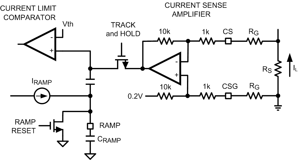
Consequently, the inductor current in buck-boost mode is much larger especially when VOUT is large relative to VIN. The LM25118 provides a current monitoring scheme to protect the circuit from possible overcurrent conditions. When set correctly, the emulated current sense signal is proportional to the buck switch current with a scale factor determined by the current sense resistor. The emulated ramp signal is applied to the current limit comparator. If the peak of the emulated ramp signal exceeds 1.25 V when operating in the buck mode, the PWM cycle is immediately terminated (cycle-by-cycle current limiting). In buck-boost mode the current limit threshold is increased to 2.50 V to allow higher peak inductor current. To further protect the external switches during prolonged overload conditions, an internal counter detects consecutive cycles of current limiting. If the counter detects 256 consecutive current limited PWM cycles, the LM25118 enters a low power dissipation hiccup mode. In the hiccup mode, the output drivers are disabled, the UVLO pin is momentarily pulled low, and the soft-start capacitor is discharged. The regulator is restarted with a normal soft-start sequence once the UVLO pin charges back to 1.23 V. The hiccup mode off-time can be programmed by an external capacitor connected from UVLO pin to ground. This hiccup cycle will repeat until the output overload condition is removed.
In applications with low output inductance and high input voltage, the switch current may overshoot due to the propagation delay of the current limit comparator and control circuitry. If an overshoot should occur, the sample-and-hold circuit will detect the excess recirculating diode current. If the sample-and-hold pedestal level exceeds the internal current limit threshold, the buck switch will be disabled and will skip PWM cycles until the inductor current has decayed below the current limit threshold. This approach prevents current runaway conditions due to propagation delays or inductor saturation since the inductor current is forced to decay before the buck switch is turned on again.
 Figure 14. Current Limit and Ramp Circuit