JAJSDG8F July 2011 – March 2018 LM25118
PRODUCTION DATA.
- 1 特長
- 2 アプリケーション
- 3 概要
- 4 改訂履歴
- 5 Pin Configuration and Functions
- 6 Specifications
- 7 Detailed Description
-
8 Application and Implementation
- 8.1 Application Information
- 8.2
Typical Application
- 8.2.1 Design Requirements
- 8.2.2
Detailed Design Procedure
- 8.2.2.1 Custom Design With WEBENCH® Tools
- 8.2.2.2 R7 = RT
- 8.2.2.3 Inductor Selection – L1
- 8.2.2.4 R13 = RSENSE
- 8.2.2.5 C15 = CRAMP
- 8.2.2.6 Inductor Current Limit Calculation
- 8.2.2.7 C9 - C12 = Output Capacitors
- 8.2.2.8 D1
- 8.2.2.9 D4
- 8.2.2.10 C1 – C5 = Input Capacitors
- 8.2.2.11 C20
- 8.2.2.12 C8
- 8.2.2.13 C16 = CSS
- 8.2.2.14 R8, R9
- 8.2.2.15 R1, R3, C21
- 8.2.2.16 R2
- 8.2.2.17 Snubber
- 8.2.2.18 Error Amplifier Configuration
- 8.2.3 Application Curves
- 9 Power Supply Recommendations
- 10Layout
- 11デバイスおよびドキュメントのサポート
- 12メカニカル、パッケージ、および注文情報
パッケージ・オプション
メカニカル・データ(パッケージ|ピン)
- PWP|20
サーマルパッド・メカニカル・データ
- PWP|20
発注情報
7.4.3 High Voltage Start-Up Regulator
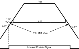
The LM25118 contains a dual-mode, high voltage linear regulator that provides the VCC bias supply for the PWM controller and the MOSFET gate driver. The VIN input pin can be connected directly to input voltages as high as 42 V. For input voltages below 10 V, an internal low dropout switch connects VCC directly to VIN. In this supply range, VCC is approximately equal to VIN. For VIN voltages greater than 10 V, the low dropout switch is disabled and the VCC regulator is enabled to maintain VCC at approximately 7 V. A wide operating range of 4 V to 42 V (with a startup requirement of at least 5 V) is achieved through the use of this dual-mode regulator.
The output of the VCC regulator is current limited to 35 mA, typical. Upon power up, the regulator sources current into the capacitor connected to the VCC pin. When the voltage at the VCC pin exceeds the VCC under-voltage threshold of 3.7 V and the UVLO input pin voltage is greater than 1.23 V, the gate driver outputs are enabled and a soft-start sequence begins. The gate driver outputs remain enabled until VCC falls below 3.5 V or the voltage at the UVLO pin falls below 1.13 V.
In many applications, the regulated output voltage or an auxiliary supply voltage can be applied to the VCCX pin to reduce the IC power dissipation. For output voltages between 4 V and 15 V, VOUT can be connected directly to VCCX. When the voltage at the VCCX pin is greater than 3.85 V, the internal VCC regulator is disabled and an internal switch connects VCCX to VCC, reducing the internal power dissipation.
In high voltage applications, take extra care to ensure the VIN pin voltage does not exceed the absolute maximum voltage rating of 45 V. During line or load transients, voltage ringing on the VIN line that exceeds the absolute maximum rating can damage the IC. Both careful PCB layout and the use of quality bypass capacitors located close to the VIN and GND pins are essential.
 Figure 17. VIN and VCC Sequencing