JAJSJI4B December 2020 – December 2021 LM25149
PRODUCTION DATA
- 1 特長
- 2 アプリケーション
- 3 概要
- 4 Revision History
- 5 概要 (続き)
- 6 Pin Configuration and Functions
- 7 Specifications
-
8 Detailed Description
- 8.1 Overview
- 8.2 Functional Block Diagram
- 8.3
Feature Description
- 8.3.1 Input Voltage Range (VIN)
- 8.3.2 High-Voltage Bias Supply Regulator (VCC, VCCX, VDDA)
- 8.3.3 Precision Enable (EN)
- 8.3.4 Power-Good Monitor (PG)
- 8.3.5 Switching Frequency (RT)
- 8.3.6 Active EMI Filter
- 8.3.7 Dual Random Spread Spectrum (DRSS)
- 8.3.8 Soft Start
- 8.3.9 Output Voltage Setpoint (FB)
- 8.3.10 Minimum Controllable On Time
- 8.3.11 Error Amplifier and PWM Comparator (FB, EXTCOMP)
- 8.3.12 Slope Compensation
- 8.3.13 Inductor Current Sense (ISNS+, VOUT)
- 8.3.14 Hiccup Mode Current Limiting
- 8.3.15 High-Side and Low-Side Gate Drivers (HO, LO)
- 8.3.16 Output Configurations (CNFG)
- 8.3.17 Single-Output Dual-Phase Operation
- 8.4 Device Functional Modes
-
9 Application and Implementation
- 9.1 Application Information
- 9.2
Typical Applications
- 9.2.1
Design 1 – High Efficiency 2.1-MHz Synchronous
Buck Regulator
- 9.2.1.1 Design Requirements
- 9.2.1.2
Detailed Design Procedure
- 9.2.1.2.1 Custom Design With WEBENCH® Tools
- 9.2.1.2.2 Custom Design With Excel Quickstart Tool
- 9.2.1.2.3 Buck Inductor
- 9.2.1.2.4 Current-Sense Resistance
- 9.2.1.2.5 Output Capacitors
- 9.2.1.2.6 Input Capacitors
- 9.2.1.2.7 Frequency Set Resistor
- 9.2.1.2.8 Feedback Resistors
- 9.2.1.2.9 Compensation Components
- 9.2.1.2.10 Active EMI Components
- 9.2.1.3 Application Curves
- 9.2.2 Design 2 – High Efficiency 440-kHz Synchronous Buck Regulator
- 9.2.3 Design 3 – Dual-Phase 400-kHz 20-A Synchronous Buck Regulator
- 9.2.1
Design 1 – High Efficiency 2.1-MHz Synchronous
Buck Regulator
- 10Power Supply Recommendations
- 11Layout
- 12Device and Documentation Support
- 13Mechanical, Packaging, and Orderable Information
パッケージ・オプション
メカニカル・データ(パッケージ|ピン)
- RGY|24
サーマルパッド・メカニカル・データ
- RGY|24
発注情報
8.3.17 Single-Output Dual-Phase Operation
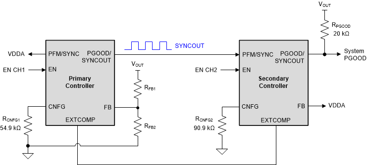
To configure for dual-phase operation, two controllers are required. The LM25149 can only be configured in a single or dual-phase configuration where both outputs are tied together. Additional phases cannot be added. Refer to Figure 8-7. Configure the first controller (CNTRL1) as a primary controller and the second controller (CNTRL2) as a secondary. To configure CNTRL1 as a primary controller, install a 54-kΩ or a 71.5-kΩ resistor from CNFG to AGND. To configure the CNTRL2 as a secondary controller, install a 90.9-kΩ resistor from CNFG to AGND. This disables the error amplifier of CNTRL2, placing it into a high-impedance state. Connect the EXTCOMP pins of the primary and secondary controllers together. The internal compensation amplifier feature is not supported when the controller is in dual-phase mode.
In dual-phase mode, the PG/SYNC pin of the primary controller becomes a SYNCOUT. Refer to the Electrical Characteristics for voltage levels. Connect PG of the primary to PFM/SYNC (SYNCIN) of the secondary controller. The PG/SYNCOUT signal of the primary controller is 180° out-of-phase and facilitates interleaved operation. RT is not used for the oscillator when the LM25149 is in secondary controller mode, but instead is used for slope compensation. Therefore, select the RT resistance to be the same as that of the primary controller. The oscillator is derived from the primary controller. When in primary/secondary mode, enable both controllers simultaneously for start-up. After the regulator has started, pull the secondary EN pin low (< 0.8 V) for phase shedding if needed at light load to increase the efficiency.Configure PFM mode by connecting the PFM/SYNC of the primary to VDDA and the FB of the secondary to VDDA as shown in Figure 8-7. Configure FPWM mode by connecting PFM/SYNC of the primary and FB of the secondary both to AGND. An external synchronization signal can be applied to the primary PFM/SYNC (SYNCIN), and the secondary FB must be configured for FPWM. If an external SYNCIN signal is applied after start-up while in primary/secondary mode, there is a two-clock cycle delay before the LM25149 locks on to the external synchronization signal.
 Figure 8-7 Schematic Configured for Single-Output
Dual-Phase Operation
Figure 8-7 Schematic Configured for Single-Output
Dual-Phase OperationPFM pulse skipping is used to reduce the IQ current and the light-load efficiency. When this occurs, the primary controller disables its synchronization clock output, so phase shedding is not supported. Phase shedding is supported in FPWM only. In FPWM, enable or disable the secondary controller as needed to support higher load current or better light-load efficiency, respectively. When the secondary is disabled and then re-enabled, its internal soft-start is pulled low and the LM25149 goes through a normal soft-start sequence.
When the LM25149 is configured for a single-output dual-phase operation using the internal 3.3-V feedback resistor divider, the internal bootstrap UV circuit can source current out of the SW pin, charging up the output capacitors approximately to 3.6 V. If this behavior is undesirable, the user can add a 100-kΩ resistor from VOUT to GND to bleed off the charge on the output capacitors.
For more information, see Benefits of a Multiphase Buck Converter technical brief and Multiphase Buck Design From Start to Finish application report.