JAJS851G April 2000 – May 2019 LM2585
PRODUCTION DATA.
- 1 特長
- 2 アプリケーション
- 3 概要
- 4 改訂履歴
- 5 Pin Configurations
-
6 Specifications
- 6.1 Absolute Maximum Ratings
- 6.2 ESD Ratings
- 6.3 Recommended Operating Ratings
- 6.4 Thermal Information
- 6.5 Electrical Characteristics: 3.3 V
- 6.6 Electrical Characteristics: 5 V
- 6.7 Electrical Characteristics: 12-V
- 6.8 Electrical Characteristics: Adjustable
- 6.9 Electrical Characteristics: All Versions
- 6.10 Typical Characteristics
- 7 Detailed Description
- 8 Application and Implementation
- 9 Layout
- 10デバイスおよびドキュメントのサポート
- 11メカニカル、パッケージ、および注文情報
パッケージ・オプション
メカニカル・データ(パッケージ|ピン)
サーマルパッド・メカニカル・データ
- KTT|5
発注情報
7.3.1 Step-Up (Boost) Regulator Operation
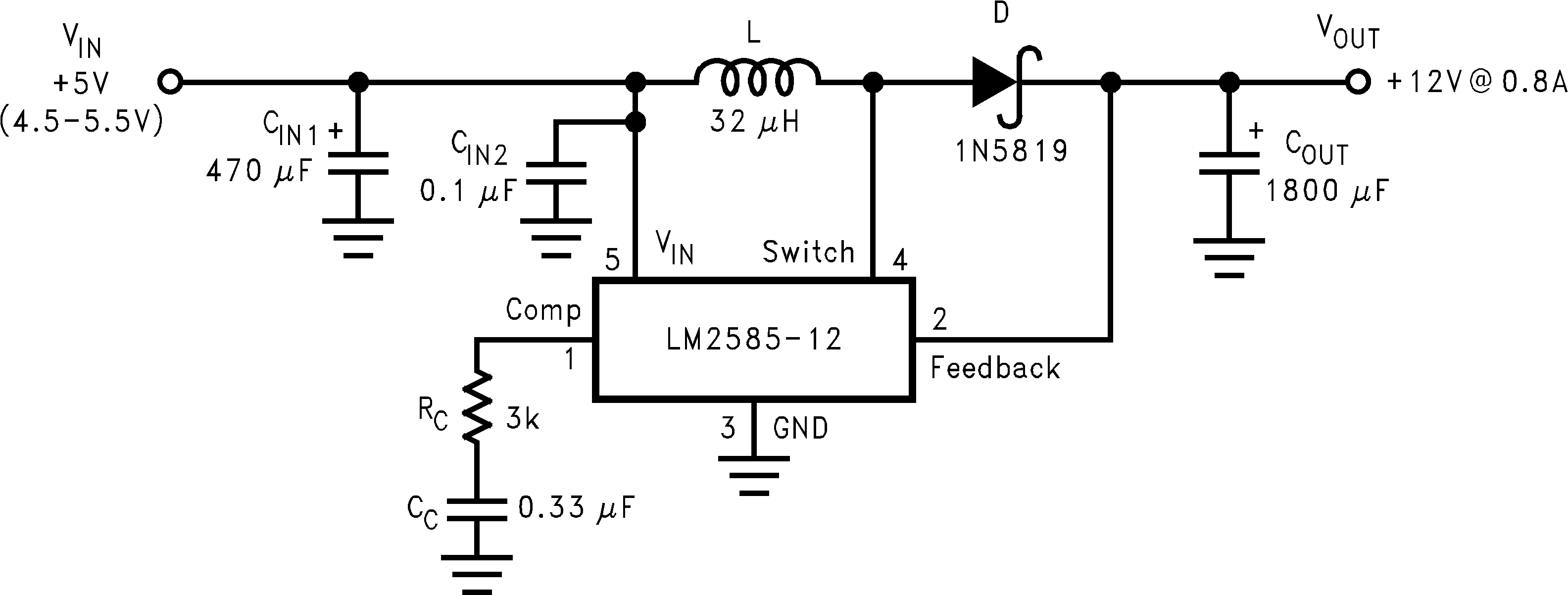
Figure 15 shows the LM2585 used as a step-up (boost) regulator. This is a switching regulator that produces an output voltage greater than the input supply voltage.
A brief explanation of how the LM2585 boost regulator works is as follows (refer to Figure 15). When the NPN switch turns on, the inductor current ramps up at the rate of VIN/L, storing energy in the inductor. When the switch turns off, the lower end of the inductor flies above VIN, discharging its current through diode (D) into the output capacitor (COUT) at a rate of (VOUT − VIN)/L. Thus, energy stored in the inductor during the switch on time is transferred to the output during the switch off time. The output voltage is controlled by adjusting the peak switch current, as described in .
 Figure 15. 12-V Boost Regulator
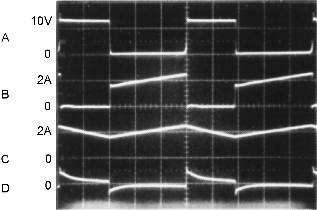
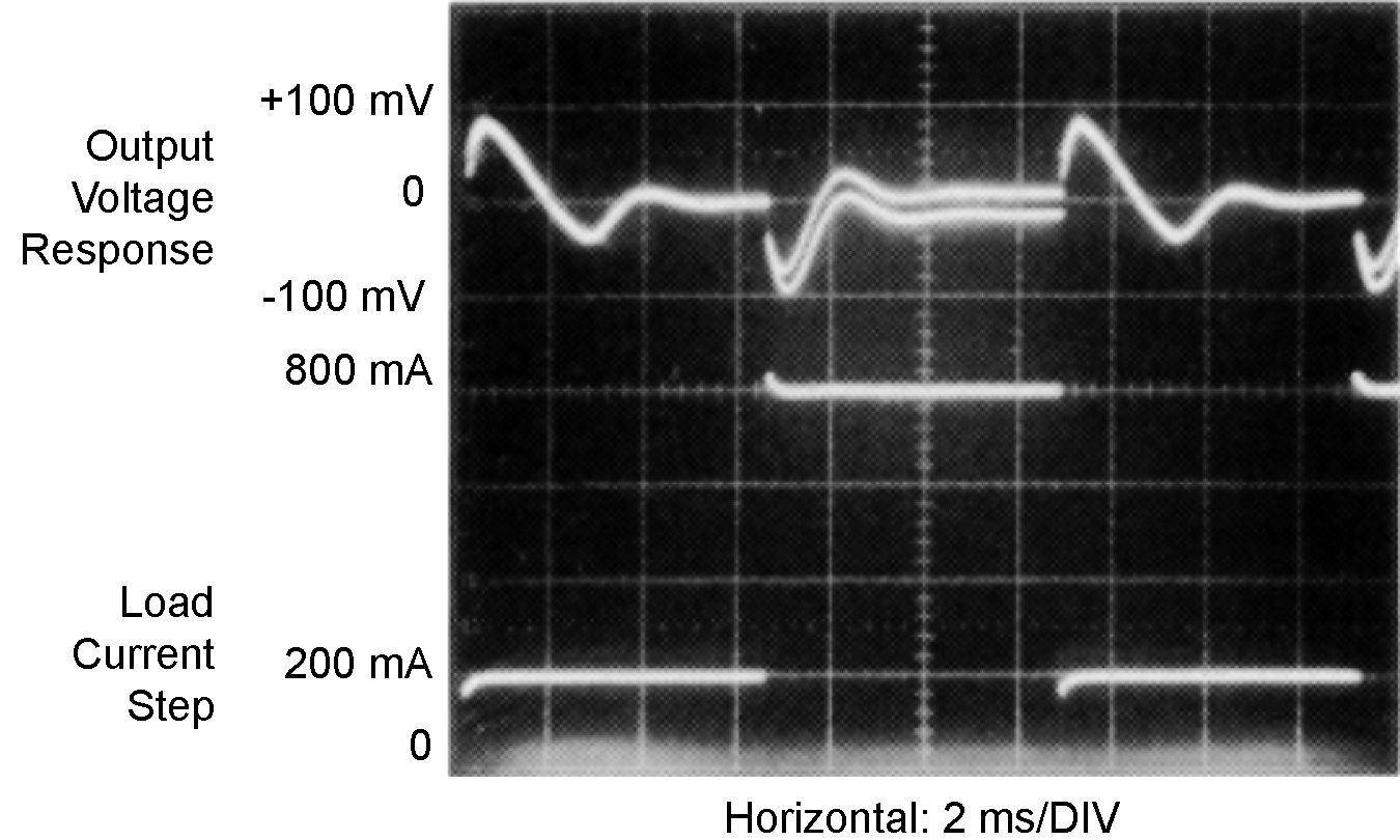
 By adding a small number of external components (as shown in Figure 15), the LM2585 can be used to produce a regulated output voltage that is greater than the applied input voltage. The switching waveforms observed during the operation of this circuit are shown in Figure 16. Typical performance of this regulator is shown in Figure 17.

B: Switch Current, 2 A/div
C: Inductor Current, 2 A/div
D: Output Ripple Voltage,
100 mV/div, AC-Coupled
Horizontal: 2 μs/div
 Figure 17. VOUT Response To Load Current Step