JAJS851G April   2000  – May 2019 LM2585

PRODUCTION DATA.  

  1. 特長
  2. アプリケーション
  3. 概要
    1.     Device Images
      1.      12V フライバック・レギュレータ設計例
  4. 改訂履歴
  5. Pin Configurations
  6. Specifications
    1. 6.1  Absolute Maximum Ratings
    2. 6.2  ESD Ratings
    3. 6.3  Recommended Operating Ratings
    4. 6.4  Thermal Information
    5. 6.5  Electrical Characteristics: 3.3 V
    6. 6.6  Electrical Characteristics: 5 V
    7. 6.7  Electrical Characteristics: 12-V
    8. 6.8  Electrical Characteristics: Adjustable
    9. 6.9  Electrical Characteristics: All Versions
    10. 6.10 Typical Characteristics
  7. Detailed Description
    1. 7.1 Overview
    2. 7.2 Functional Block Diagram
    3. 7.3 Feature Description
      1. 7.3.1 Step-Up (Boost) Regulator Operation
  8. Application and Implementation
    1. 8.1 Application Information
    2. 8.2 Typical Applications
      1. 8.2.1 Typical Boost Regulator Applications
      2. 8.2.2 Typical Flyback Regulator Applications
        1. 8.2.2.1 Transformer Selection (T)
        2. 8.2.2.2 Transformer Footprints
          1. 8.2.2.2.0.1 T6
          2. 8.2.2.2.0.2 T6
      3. 8.2.3 Design Requirements
      4. 8.2.4 Detailed Design Procedure
        1. 8.2.4.1 Custom Design With WEBENCH® Tools
        2. 8.2.4.2 Programming Output Voltage (Selecting R1 And R2)
        3. 8.2.4.3 Short Circuit Condition
        4. 8.2.4.4 Flyback Regulator Input Capacitors
        5. 8.2.4.5 Switch Voltage Limits
        6. 8.2.4.6 Output Voltage Limitations
        7. 8.2.4.7 Noisy Input Line Condition
        8. 8.2.4.8 Stability
      5. 8.2.5 Application Curve
    3. 8.3 Additional Application Examples
      1. 8.3.1 Test Circuits
  9. Layout
    1. 9.1 Layout Guidelines
    2. 9.2 Heat Sink/Thermal Considerations
  10. 10デバイスおよびドキュメントのサポート
    1. 10.1 デバイス・サポート
      1. 10.1.1 デベロッパー・ネットワークの製品に関する免責事項
      2. 10.1.2 開発サポート
        1. 10.1.2.1 WEBENCH®ツールによるカスタム設計
    2. 10.2 ドキュメントの更新通知を受け取る方法
    3. 10.3 コミュニティ・リソース
    4. 10.4 商標
    5. 10.5 静電気放電に関する注意事項
    6. 10.6 Glossary
  11. 11メカニカル、パッケージ、および注文情報

パッケージ・オプション

メカニカル・データ(パッケージ|ピン)
サーマルパッド・メカニカル・データ
発注情報

Output Voltage Limitations

The maximum output voltage of a boost regulator is the maximum switch voltage minus a diode drop. In a flyback regulator, the maximum output voltage is determined by the turns ratio, N, and the duty cycle, D, by the equation:

Equation 4. VOUT ≈ N × VIN × D/(1 − D)

The duty cycle of a flyback regulator is determined by the following equation:

Equation 5. LM2585 1251559.png

Theoretically, the maximum output voltage can be as large as desired—just keep increasing the turns ratio of the transformer. However, there exists some physical limitations that prevent the turns ratio, and thus the output voltage, from increasing to infinity. The physical limitations are capacitances and inductances in the LM2585 switch, the output diode(s), and the transformer—such as reverse recovery time of the output diode (mentioned above).
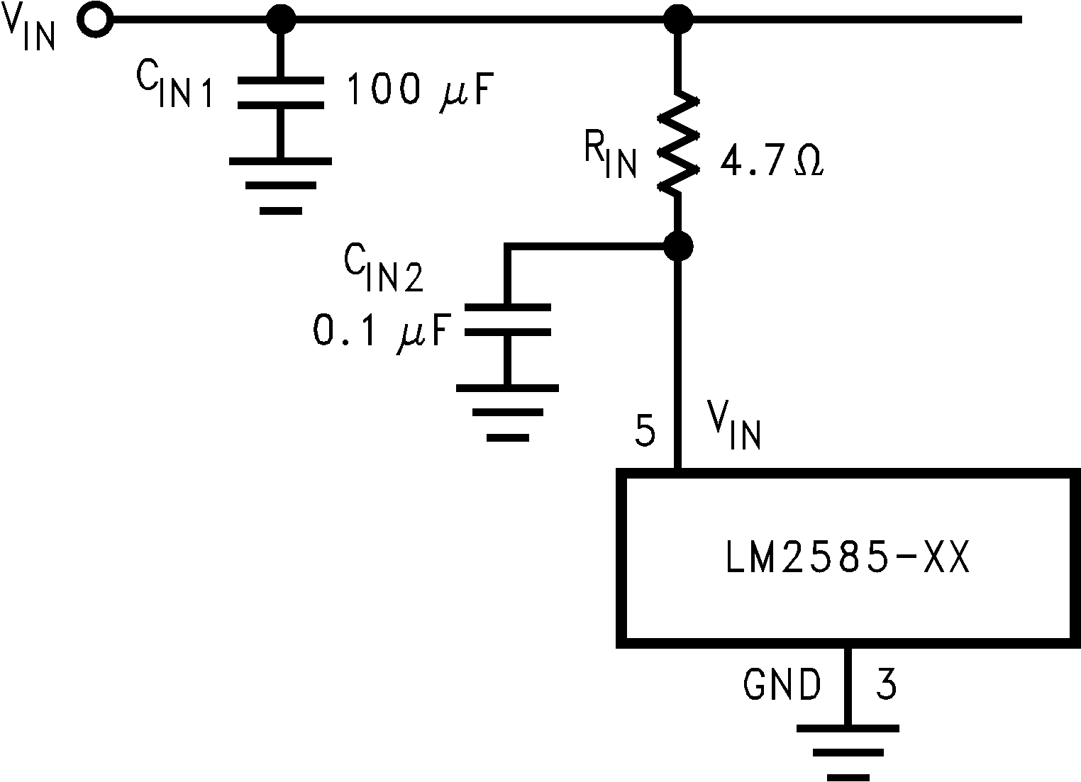
LM2585 1251557.pngFigure 44. Input Line Filter