JAJS852E May   1996  – May 2019 LM2586

PRODUCTION DATA.  

  1. 特長
  2. 代表的なアプリケーション
  3. 概要
    1.     Device Images
      1.      ブロック図
  4. 改訂履歴
  5. 概要(続き)
  6. Pin Configurations
  7. Specifications
    1. 7.1 Absolute Maximum Ratings
    2. 7.2 ESD Ratings
    3. 7.3 Recommended Operating Ratings
    4. 7.4 Thermal Information
    5. 7.5 Electrical Characteristics: 3.3 V
    6. 7.6 Electrical Characteristics: 5 V
    7. 7.7 Electrical Characteristics: 12 V
    8. 7.8 Electrical Characteristics: Adjustable
    9. 7.9 Typical Characteristics
  8. Detailed Description
    1. 8.1 Overview
    2. 8.2 Functional Block Diagram
    3. 8.3 Feature Description
      1. 8.3.1 Flyback Regulator Operation
      2. 8.3.2 Step-Up (Boost) Regulator Operation
      3. 8.3.3 Programming Output Voltage (Selecting R1 And R2)
      4. 8.3.4 Shutdown Control
      5. 8.3.5 Frequency Adjustment
      6. 8.3.6 Frequency Synchronization
  9. Application and Implementation
    1. 9.1 Application Information
    2. 9.2 Typical Applications
      1. 9.2.1 Typical Flyback Regulator Applications
        1. 9.2.1.1 Design Requirements
          1. 9.2.1.1.1 Transformer Selection (T)
          2. 9.2.1.1.2 Transformer Footprints
        2. 9.2.1.2 Detailed Design Procedure
          1. 9.2.1.2.1 Custom Design With WEBENCH® Tools
          2. 9.2.1.2.2 Flyback Regulator Input Capacitors
          3. 9.2.1.2.3 Switch Voltage Limits
          4. 9.2.1.2.4 Output Voltage Limitations
          5. 9.2.1.2.5 Noisy Input Line Condition
          6. 9.2.1.2.6 Stability
      2. 9.2.2 Typical Boost Regulator Applications
        1. 9.2.2.1 Design Requirements
        2. 9.2.2.2 Detailed Design Procedure
    3. 9.3 System Examples
      1. 9.3.1 Test Circuits
  10. 10Layout
    1. 10.1 Layout Guidelines
    2. 10.2 Layout Example
  11. 11Heat Sink/Thermal Considerations
  12. 12デバイスおよびドキュメントのサポート
    1. 12.1 デバイス・サポート
      1. 12.1.1 デベロッパー・ネットワークの製品に関する免責事項
      2. 12.1.2 開発サポート
        1. 12.1.2.1 WEBENCH®ツールによるカスタム設計
    2. 12.2 ドキュメントの更新通知を受け取る方法
    3. 12.3 コミュニティ・リソース
    4. 12.4 商標
    5. 12.5 静電気放電に関する注意事項
    6. 12.6 Glossary
  13. 13メカニカル、パッケージ、および注文情報

パッケージ・オプション

メカニカル・データ(パッケージ|ピン)
サーマルパッド・メカニカル・データ
発注情報

Flyback Regulator Operation

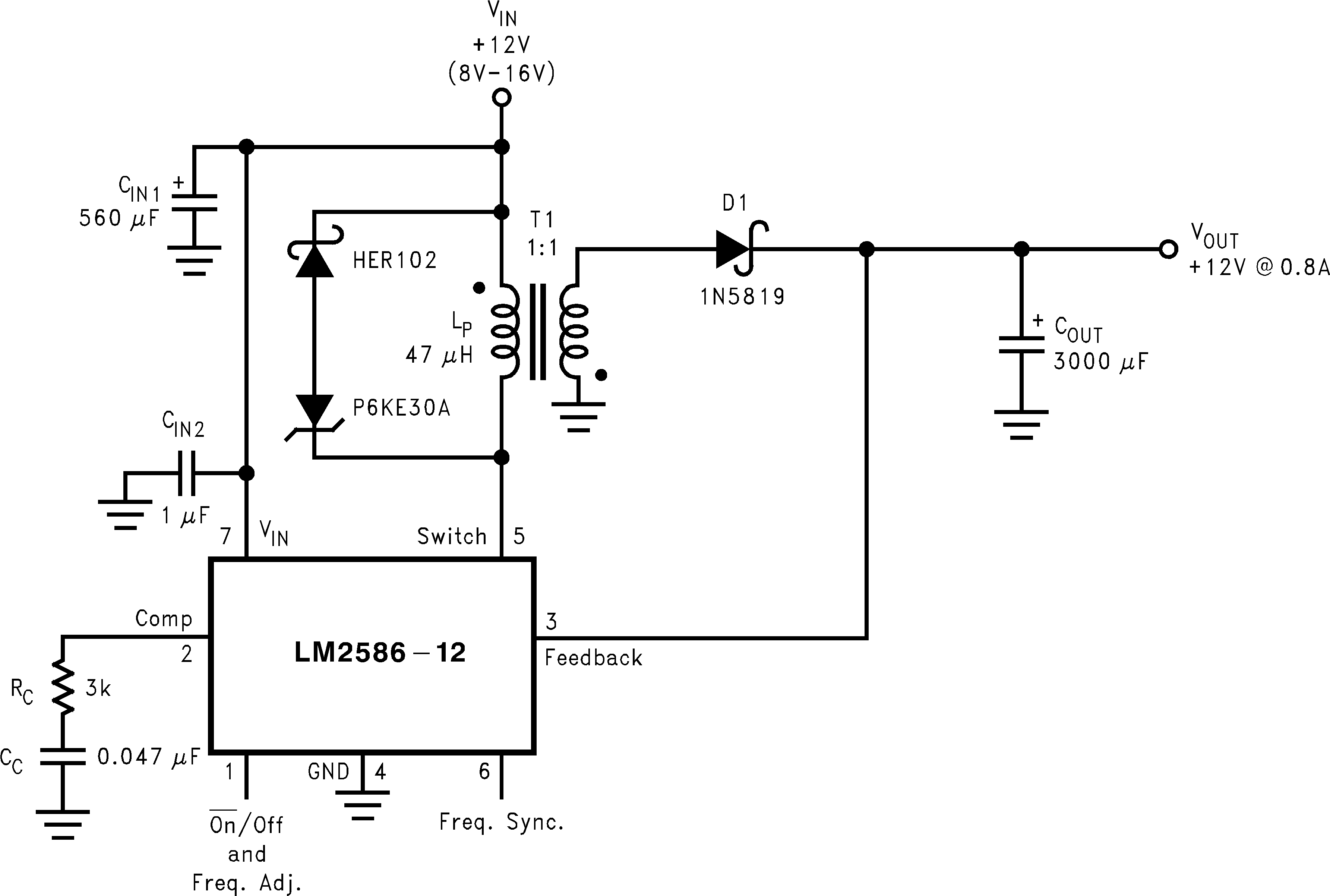
The LM2586 is ideally suited for use in the flyback regulator topology. The flyback regulator can produce a single output voltage, such as the one shown in Figure 16, or multiple output voltages. In Figure 16, the flyback regulator generates an output voltage that is inside the range of the input voltage. This feature is unique to flyback regulators and cannot be duplicated with buck or boost regulators.

The operation of a flyback regulator is as follows (refer to Figure 16): when the switch is on, current flows through the primary winding of the transformer, T1, storing energy in the magnetic field of the transformer. Note that the primary and secondary windings are out of phase, so no current flows through the secondary when current flows through the primary. When the switch turns off, the magnetic field collapses, reversing the voltage polarity of the primary and secondary windings. Now rectifier D1 is forward biased and current flows through it, releasing the energy stored in the transformer. This produces voltage at the output.

The output voltage is controlled by modulating the peak switch current. This is done by feeding back a portion of the output voltage to the error amp, which amplifies the difference between the feedback voltage and a 1.230V reference. The error amp output voltage is compared to a ramp voltage proportional to the switch current (in other words, inductor current during the switch on time). The comparator terminates the switch on time when the two voltages are equal, thereby controlling the peak switch current to maintain a constant output voltage.
LM2586 01251624.png
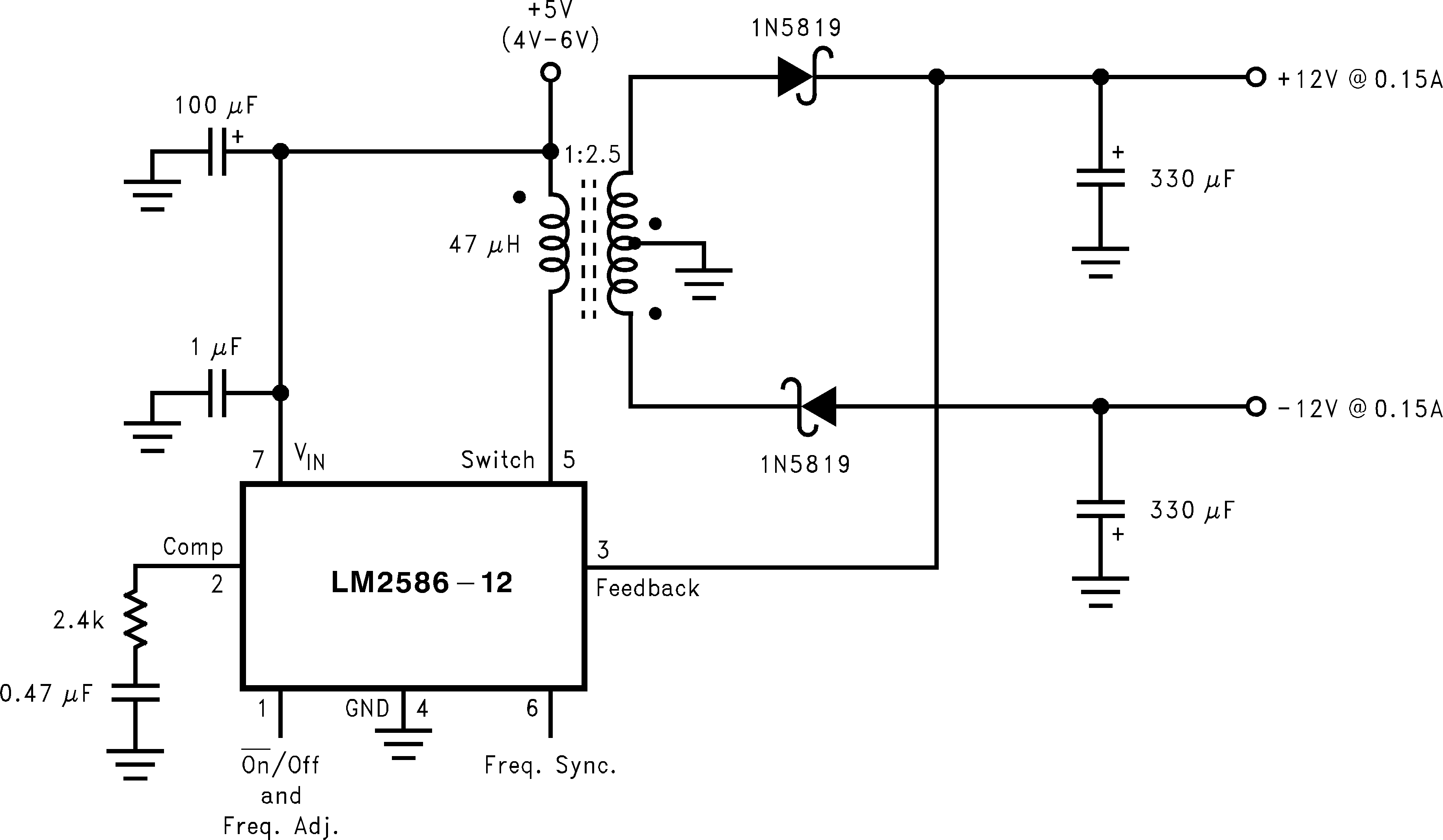
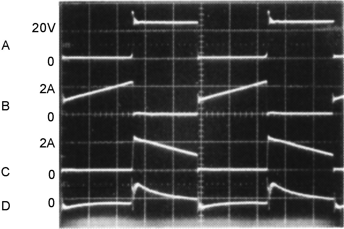
As shown in Figure 16, the LM2586 can be used as a flyback regulator by using a minimum number of external components. The switching waveforms of this regulator are shown in . Typical performance characteristics observed during the operation of this circuit are shown in .
Figure 16. 12-V Flyback Regulator Design Example
LM2586 1251521.pngFigure 17. 12-V Flyback Regulator Design Example
LM2586 01251601.png
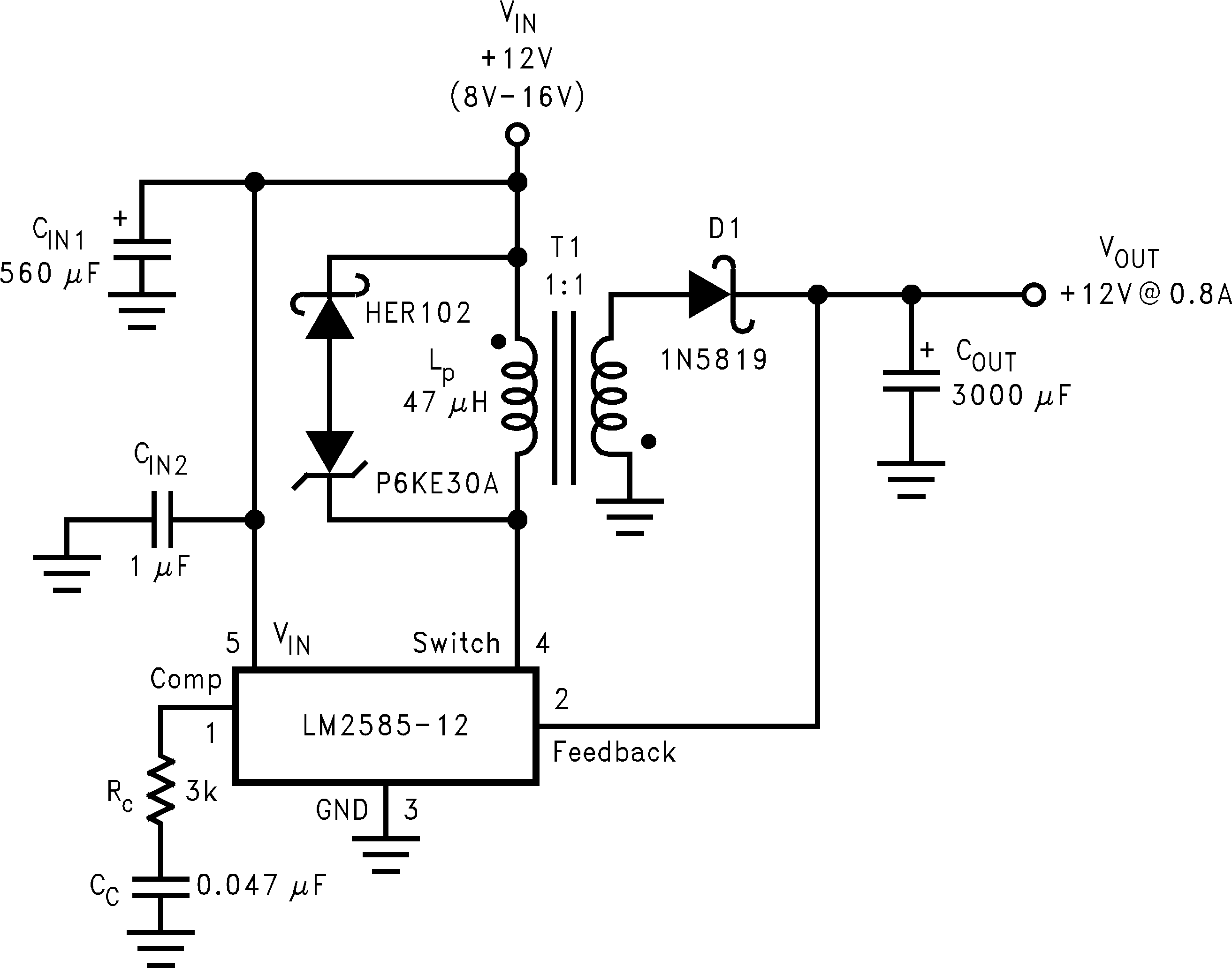
As shown in Figure 17, the LM2585 can be used as a flyback regulator by using a minimum number of external components. The switching waveforms of this regulator are shown in Figure 18. Typical characteristics observed during the operation of this circuit are shown in Figure 19.
LM2586 1251522.png
A: Switch Voltage, 20 V/div

B: Switch Current, 2 A/div

C: Output Rectifier Current, 2 A/div

D: Output Ripple Voltage, 50 mV/div

AC-Coupled

Horizontal: 2 μs/div
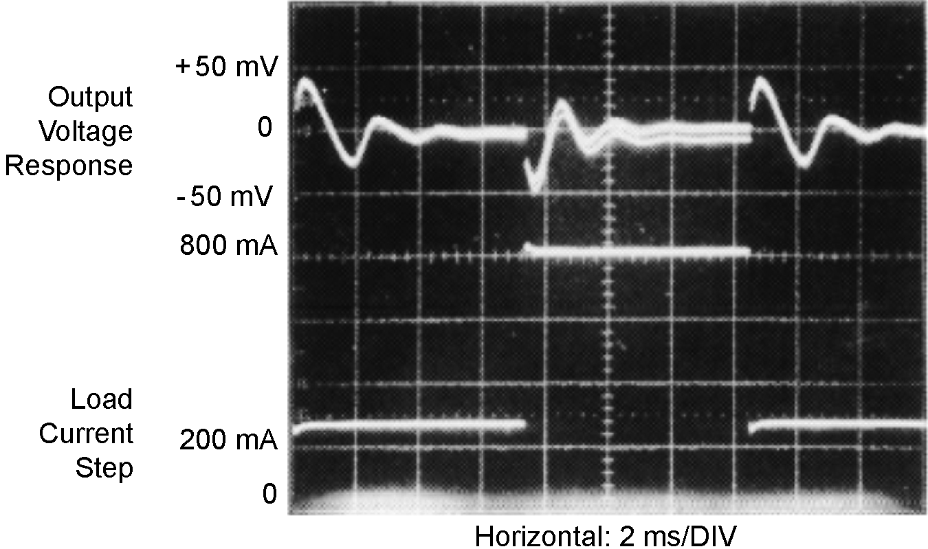
Figure 18. Switching Waveforms
LM2586 1251523.png
Figure 19. VOUT Load Current Step Response