JAJS852E May   1996  – May 2019 LM2586

PRODUCTION DATA.  

  1. 特長
  2. 代表的なアプリケーション
  3. 概要
    1.     Device Images
      1.      ブロック図
  4. 改訂履歴
  5. 概要(続き)
  6. Pin Configurations
  7. Specifications
    1. 7.1 Absolute Maximum Ratings
    2. 7.2 ESD Ratings
    3. 7.3 Recommended Operating Ratings
    4. 7.4 Thermal Information
    5. 7.5 Electrical Characteristics: 3.3 V
    6. 7.6 Electrical Characteristics: 5 V
    7. 7.7 Electrical Characteristics: 12 V
    8. 7.8 Electrical Characteristics: Adjustable
    9. 7.9 Typical Characteristics
  8. Detailed Description
    1. 8.1 Overview
    2. 8.2 Functional Block Diagram
    3. 8.3 Feature Description
      1. 8.3.1 Flyback Regulator Operation
      2. 8.3.2 Step-Up (Boost) Regulator Operation
      3. 8.3.3 Programming Output Voltage (Selecting R1 And R2)
      4. 8.3.4 Shutdown Control
      5. 8.3.5 Frequency Adjustment
      6. 8.3.6 Frequency Synchronization
  9. Application and Implementation
    1. 9.1 Application Information
    2. 9.2 Typical Applications
      1. 9.2.1 Typical Flyback Regulator Applications
        1. 9.2.1.1 Design Requirements
          1. 9.2.1.1.1 Transformer Selection (T)
          2. 9.2.1.1.2 Transformer Footprints
        2. 9.2.1.2 Detailed Design Procedure
          1. 9.2.1.2.1 Custom Design With WEBENCH® Tools
          2. 9.2.1.2.2 Flyback Regulator Input Capacitors
          3. 9.2.1.2.3 Switch Voltage Limits
          4. 9.2.1.2.4 Output Voltage Limitations
          5. 9.2.1.2.5 Noisy Input Line Condition
          6. 9.2.1.2.6 Stability
      2. 9.2.2 Typical Boost Regulator Applications
        1. 9.2.2.1 Design Requirements
        2. 9.2.2.2 Detailed Design Procedure
    3. 9.3 System Examples
      1. 9.3.1 Test Circuits
  10. 10Layout
    1. 10.1 Layout Guidelines
    2. 10.2 Layout Example
  11. 11Heat Sink/Thermal Considerations
  12. 12デバイスおよびドキュメントのサポート
    1. 12.1 デバイス・サポート
      1. 12.1.1 デベロッパー・ネットワークの製品に関する免責事項
      2. 12.1.2 開発サポート
        1. 12.1.2.1 WEBENCH®ツールによるカスタム設計
    2. 12.2 ドキュメントの更新通知を受け取る方法
    3. 12.3 コミュニティ・リソース
    4. 12.4 商標
    5. 12.5 静電気放電に関する注意事項
    6. 12.6 Glossary
  13. 13メカニカル、パッケージ、および注文情報

パッケージ・オプション

メカニカル・データ(パッケージ|ピン)
サーマルパッド・メカニカル・データ
発注情報

Frequency Synchronization

Another feature of the LM2586 is the ability to synchronize the switching frequency to an external source, using the sync pin (pin 6). This feature allows the user to parallel multiple devices to deliver more output power.

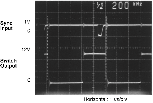
A negative falling pulse applied to the sync pin will synchronize the LM2586 to an external oscillator (see Figure 24 and Figure 25).

Use of this feature enables the LM2586 to be synchronized to an external oscillator, such as a system clock. This operation allows multiple power supplies to operate at the same frequency, thus eliminating frequency-related noise problems.

LM2586 01251659.pngFigure 24. Frequency Synchronization
LM2586 01251669.pngFigure 25. Waveforms of a Synchronized 12-V Boost Regulator

The scope photo in Figure 25 shows a LM2586 12-V boost regulator synchronized to a 200-kHz signal. There is a 700-ns delay between the falling edge of the sync signal and the turning on of the switch.
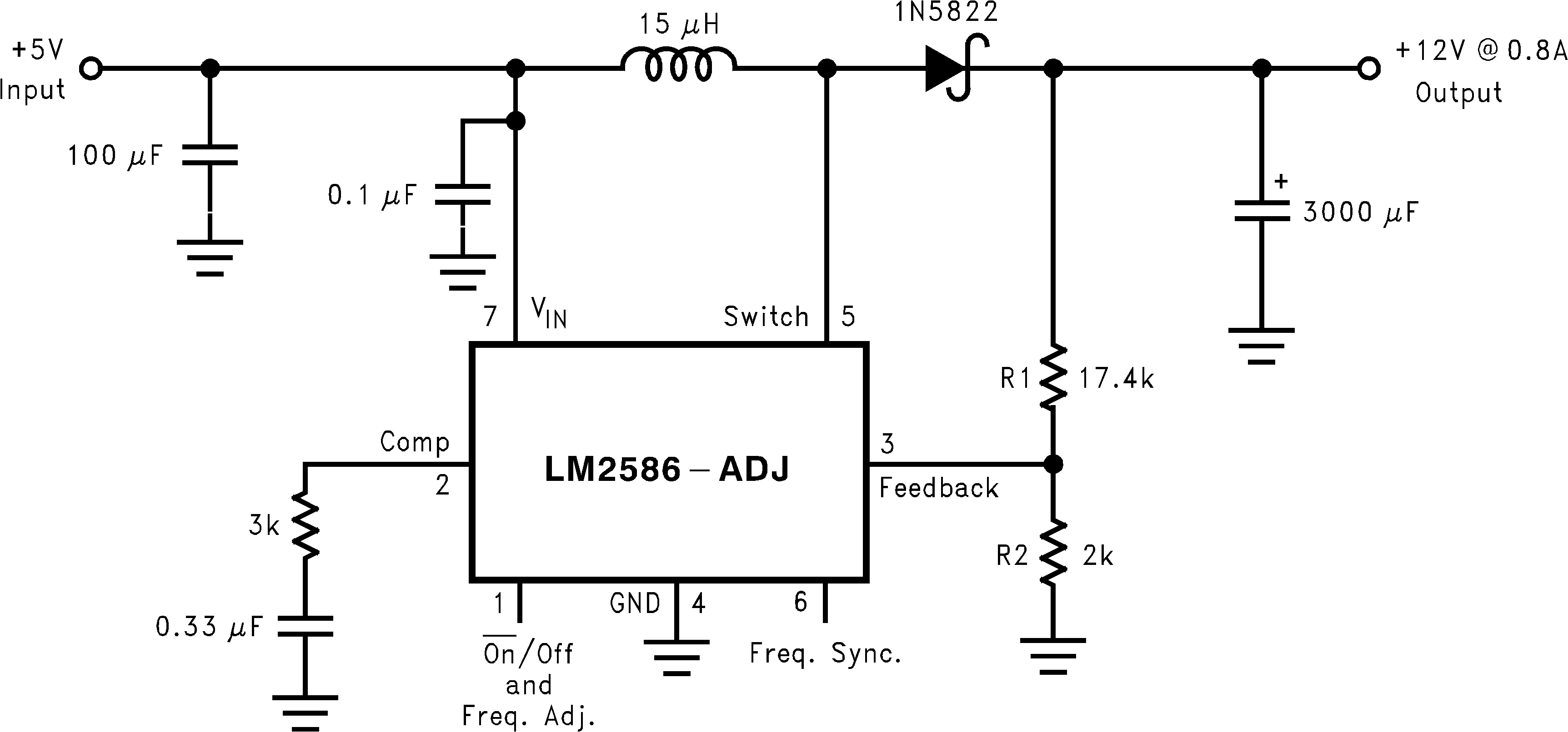
LM2586 01251661.pngFigure 26. Boost Regulator