JAJS857D March 1998 – May 2016 LM2598
PRODUCTION DATA.
- 1 特長
- 2 アプリケーション
- 3 概要
- 4 改訂履歴
- 5 概要(続き)
- 6 Pin Configuration and Functions
-
7 Specifications
- 7.1 Absolute Maximum Ratings
- 7.2 ESD Ratings
- 7.3 Recommended Operating Conditions
- 7.4 Thermal Information
- 7.5 Electrical Characteristics - 3.3-V Version
- 7.6 Electrical Characteristics - 5-V Version
- 7.7 Electrical Characteristics - 12-V Version
- 7.8 Electrical Characteristics - Adjustable Voltage Version
- 7.9 Electrical Characteristics - All Output Voltage Versions
- 7.10 Typical Characteristics
- 8 Detailed Description
- 9 Application and Implementation
- 10Power Supply Recommendations
- 11Layout
- 12デバイスおよびドキュメントのサポート
- 13メカニカル、パッケージ、および注文情報
パッケージ・オプション
メカニカル・データ(パッケージ|ピン)
サーマルパッド・メカニカル・データ
- KTW|7
発注情報
6 Pin Configuration and Functions
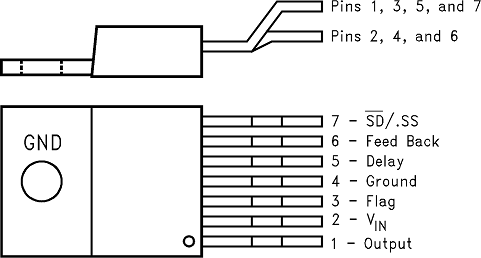
NDZ Package
7-Pin TO-220
Top View

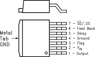
KTW Package
7-Pin TO-263
Top View

Pin Functions
| PIN | I/O | DESCRIPTION | |
|---|---|---|---|
| NO. | NAME | ||
| 1 | Output | O | Internal switch. The voltage at this pin switches between approximately (+VIN – VSAT) and approximately –0.5 V, with a duty cycle of VOUT / VIN. To minimize coupling to sensitive circuitry, the PCB copper area connected to this pin must be kept to a minimum. |
| 2 | +VIN | I | This is the positive input supply for the IC switching regulator. A suitable input bypass capacitor must be present at this pin to minimize voltage transients and to supply the switching currents required by the regulator. |
| 3 | Error Flag | O | Open collector output that provides a low signal (flag transistor ON) when the regulated output voltage drops more than 5% from the nominal output voltage. On start up, Error Flag is low until VOUT reaches 95% of the nominal output voltage and a delay time determined by the Delay pin capacitor. This signal can be used as a reset to a microprocessor on power-up.(1) |
| 4 | Ground | — | Circuit ground. |
| 5 | Delay | O | At power-up, this pin can be used to provide a time delay between the time the regulated output voltage reaches 95% of the nominal output voltage, and the time the error flag output goes high.(1) |
| 6 | Feedback | I | Senses the regulated output voltage to complete the feedback loop. |
| 7 | Shutdown/Soft-start | I | This dual function pin provides the following features: (a) Allows the switching regulator circuit to be shut down using logic level signals thus dropping the total input supply current to approximately 80 μA. (b) Adding a capacitor to this pin provides a soft-start feature which minimizes start-up current and provides a controlled ramp up of the output voltage.(1) |
(1) If any of the above three features (Shutdown/Soft-start, Error Flag, or Delay) are not used, the respective pins must be left open.