SNOS965J June   2001  – December 2015 LM2611

PRODUCTION DATA.  

  1. Features
  2. Applications
  3. Description
  4. Revision History
  5. Pin Configuration and Functions
  6. Specifications
    1. 6.1 Absolute Maximum Ratings
    2. 6.2 ESD Ratings
    3. 6.3 Recommended Operating Conditions
    4. 6.4 Thermal Information
    5. 6.5 Electrical Characteristics
  7. Detailed Description
    1. 7.1 Overview
    2. 7.2 Functional Block Diagram
    3. 7.3 Feature Description
      1. 7.3.1 Cuk Converter
      2. 7.3.2 Output and Input Inductor
      3. 7.3.3 Switch Current Limit
      4. 7.3.4 Input Capacitor
      5. 7.3.5 Output Capacitor
      6. 7.3.6 Improving Transient Response and Compensation
    4. 7.4 Device Functional Modes
      1. 7.4.1 Hysteretic Mode
        1. 7.4.1.1 Thermal Shutdown
  8. Application and Implementation
    1. 8.1 Application Information
    2. 8.2 Typical Application
      1. 8.2.1 Cuk Converter With Integrated Switch
        1. 8.2.1.1 Design Requirements
        2. 8.2.1.2 Detailed Design Procedure
        3. 8.2.1.3 Application Curves
      2. 8.2.2 5-V to -5-V Inverting Converter
        1. 8.2.2.1 Design Requirements
        2. 8.2.2.2 Application Curves
      3. 8.2.3 9-V to -5-V Inverting Converter
        1. 8.2.3.1 Design Requirements
        2. 8.2.3.2 Application Curve
      4. 8.2.4 12-V to -5-V Inverting Converter
        1. 8.2.4.1 Design Requirements
        2. 8.2.4.2 Application Curve
      5. 8.2.5 LM2611 Operating With Separate Power and Biasing Supplies
        1. 8.2.5.1 Design Requirements
        2. 8.2.5.2 Detailed Design Procedure
          1. 8.2.5.2.1 Split Supply Operation
      6. 8.2.6 Shutdown and Soft-Start
        1. 8.2.6.1 Design Requirements
        2. 8.2.6.2 Detailed Design Procedure
          1. 8.2.6.2.1 Shutdown and Soft-Start
        3. 8.2.6.3 Application Curves
      7. 8.2.7 High Duty Cycle and Load Current
        1. 8.2.7.1 Design Requirements
        2. 8.2.7.2 Detailed Design Procedure
          1. 8.2.7.2.1 High Duty Cycle and Load Current Operation
  9. Power Supply Recommendations
  10. 10Layout
    1. 10.1 Layout Guidelines
    2. 10.2 Layout Example
  11. 11Device and Documentation Support
    1. 11.1 Community Resources
    2. 11.2 Trademarks
    3. 11.3 Electrostatic Discharge Caution
    4. 11.4 Glossary
  12. 12Mechanical, Packaging, and Orderable Information

パッケージ・オプション

メカニカル・データ(パッケージ|ピン)
サーマルパッド・メカニカル・データ
発注情報

1 Features

  • 1.4-MHz Switching Frequency
  • Low RDS(ON) DMOS FET
  • 1-mVp-p Output Ripple
  • −5 V at 300 mA From 5-V Input
  • Better Regulation Than a Charge Pump
  • Uses Tiny Capacitors and Inductors
  • Wide Input Range: 2.7 V to 14 V
  • Low Shutdown Current: <1 µA
  • 5-Pin SOT-23 Package

2 Applications

  • MR Head Bias
  • Digital Camera CCD Bias
  • LCD Bias
  • GaAs FET Bias
  • Positive to Negative Conversion

3 Description

The LM2611 is a current mode, PWM inverting switching regulator. Operating from a 2.7-V to 4-V supply, it is capable of producing a regulated negative output voltage of up to −(36 VIN(MAX)). The LM2611 utilizes an input and output inductor, which enables low voltage ripple and RMS current on both the input and the output. With a switching frequency of 1.4 MHz, the inductors and output capacitor can be physically small and low cost. High efficiency is achieved through the use of a low RDS(ON) FET.

The LM2611 features a shutdown pin, which can be activated when the part is not needed to lower the Iq and save battery life. A negative feedback (NFB) pin provides a simple method of setting the output voltage, using just two resistors. Cycle-by-cycle current limiting and internal compensation further simplify the use of the LM2611.

The LM2611 is available as a small 5-pin, SOT-23 package and comes in two grades. Grade A has a 1.2-A current limit and 0.5-Ω RDS(ON), and Grade B has a 0.9-A current limit and 0.7-Ω RDS(ON).

Device Information(1)

PART NUMBER PACKAGE BODY SIZE (NOM)
LM2611 SOT-23 (5) 1.60 mm × 2.90 mm
  1. For all available packages, see the orderable addendum at the end of the data sheet.

Typical Application Circuit
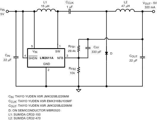
LM2611 20018117.gif