SNVS457D February 2007 – October 2015 LM26400Y
PRODUCTION DATA.
7 Detailed Description
7.1 Overview
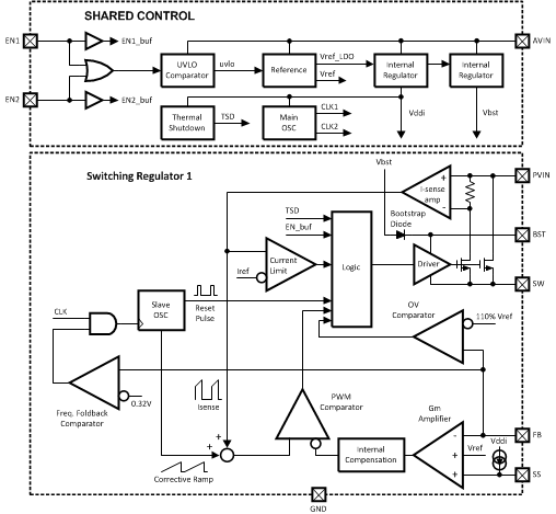
The LM26400Y device is a dual PWM peak-current mode buck regulator with two integrated power MOSFET switches. The part is designed to be easy to use. The two regulators are mostly identical and share the same input voltage and the same reference voltage (0.6 V). The two PWM clocks are of the same frequency but 180° out of phase. The two channels can have different soft-start ramp slopes and can be turned on and off independently.
Loop compensation is built in. The feedback loop design is optimized for ceramic output capacitors.
Since the power switches are built in, the achievable output current level also has to do with thermal environment of the specific application. The LM26400Y enters thermal shutdown when the junction temperature exceeds approximately 165°C.
7.2 Functional Block Diagram

7.3 Feature Description
7.3.1 Overcurrent Protection
The instantaneous switch current is limited to a typical of 3 Amperes. Any time the switch current reaches that value, the switch will be turned off immediately. This will result in a smaller duty cycle than normal, which will cause the output voltage to dip. The output voltage will continue drooping until the load draws a current that is equal to the peak-limited inductor current. As the output voltage droops, the FB pin voltage will also droop proportionally. When the FB voltage dips below 0.35 V or so, the PWM frequency will start to decrease. The lower the FB voltage the lower the PWM frequency. See Figure 10.
The frequency foldback helps two things. One is to prevent the switch current from running away as a result of the finite minimum ON-time (40 ns or so for the LM26400Y) and the small duty cycle caused by lowered output voltage due to the current limit. The other is it also helps reduce thermal stress both in the IC and the external diode.
The current limit threshold of the LM26400Y remains constant over all duty cycles.
One thing to pay attention to is that recovery from an overcurrent condition does not go through a soft-start process. This is because the reference voltage at the noninverting input of the error amplifier always sits at 0.6 V during the overcurrent protection. So if the overcurrent condition is suddenly removed, the regulator will bring the FB voltage back to 0.6 V as quickly as possible. This may cause an overshoot in the output voltage. Generally, the larger the inductor or the lower the output capacitance the more the overshoot, and vice versa. If the amount of such overshoot exceeds the allowed limit for a system, add a CFF capacitor in parallel with the upper feedback resistor to eliminate the overshoot. See Load Step Response for more details on CFF.
When one channel gets into overcurrent protection mode, the operation of the other channel will not be affected.
7.3.2 Loop Stability
To the first order approximation, the LM26400Y has a VFB-to-Inductor Current transfer admittance (that is, ratio of inductor current to FB pin voltage, in frequency domain) close to the plot in Figure 24. The transfer admittance has a DC value of 104 dBS (dBS stands for decibel Siemens. The equivalent of 0 dBS is 1 Siemens.). There is a pole at 1 Hz and a zero at approximately 8 kHz. The plateau after the 8 kHz zero is about 27 dBS. There are also high frequency poles that are not shown in the figure. They include a double pole at 1.2 MHz or so, and another double pole at half the switching frequency. Depending on factors such as inductor ripple size and duty cycle, the double pole at half the switching frequency may become two separate poles near half the switching frequency.
 Figure 24. VFB-to-Inductor Current Transfer Admittance
An easy strategy to build a stable loop with reasonable phase margin is to try to cross over from 20 kHz to 100 kHz, assuming the output capacitor is ceramic. When using pure ceramic capacitors at the output, simply use the following equation to find out the crossover frequency.

where
- 22S (22 Siemens) is the equivalent of the 27 dBS transfer admittance
- r is the ratio of 0.6 V to the output voltage
Use the same equation to find out the needed output capacitance for a given crossover frequency. Phase margin is typically between 50° and 60°. The above equation is only good for a crossover from 20 kHz to 100 kHz. A crossover frequency outside this range may result in lower phase margin and less accurate prediction by the above equation.
Example: VOUT = 2.5 V, COUT = 36 µF, find out the crossover frequency.
Assume the crossover is from 20 kHz to 100 kHz. Then:

The above analysis serves as a starting point. It is a good practice to always verify loop gain on bench.
7.3.3 Load Step Response
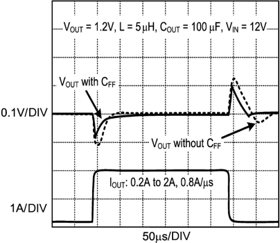
In general, the excursion in output voltage caused by a load step can be reduced by increasing the output capacitance. Besides that, increasing the small-signal loop bandwidth also helps. This can be achieved by adding a 27 nF or so capacitor (CFF) in parallel with the upper feedback resistor (assuming the lower feedback resistor is 5.9 kΩ). See Figure 25 for an illustration.
 Figure 25. Adding a CFF Capacitor
The responses to a load step from 0.2 A to 2 A with and without a CFF are shown in Figure 26. The higher loop bandwidth as a result of CFF reduces the total output excursion by about 80 mV.
 Figure 26. CFF Improves Load Step Response
Use the following equation to calculate the new loop bandwidth:

Again, the assumption is the crossover is from 20 kHz to 100 kHz.
In an extreme case where the load goes to less than 100 mA during a large load step, output voltage may exhibit extra undershoot. This usually happens when the load toggles high at the time VOUT just ramps down to its regulation level from an overshoot. Figure 27 shows such a case where the load toggles between 1.7 A and only 50 mA.
 Figure 27. Extreme Load Step
In the example, the load first goes down to 50 mA quickly (0.9 A/µs), causing a 90-µs no-switching period, and then quickly goes up to 1.7 A when VOUT1 just hits its regulation level (1.2 V), resulting in a large dip of 440 mV in the output voltage.
If it is known in a system design that the load can go down to less than 100 mA during a load step, and that the load can toggle high any time after it toggles low, take the following measures to minimize the potential extra undershoot. First is to add the Cff mentioned above. Second is to increase the output capacitance.
For example, to meet a ±10% VOUT excursion requirement for a 100 mA to 2-A load step, approximately 200 µF output capacitance is needed for a 1.2-V output, and about 44 µF is needed for a 5-V output.
7.4 Device Functional Modes
7.4.1 Start-Up and Shutdown
During a soft start, the ramp of the output voltage is proportional to the ramp of the SS pin. When the EN pin is pulled high, an internal 16-µA current source starts to charge the corresponding SS pin. The capacitance between the SS pin and ground determines how fast the SS voltage ramps up. The noninverting input of the transconductance error amplifier, that is, the moving reference during soft start, will be the lower of SS voltage and the 0.6-V reference (VREF). So before SS reaches 0.6V, the reference to the error amplifier will be the SS voltage. When SS exceeds 0.6 V, the noninverting input of the transconductance amplifier will be a constant 0.6 V and that will be the time soft start ends. The SS voltage will continue to ramp all the way up to the internal 2.7-V supply voltage before leveling off.
To calculate the needed SS capacitance for a given soft-start duration, use Equation 4.

where
- ISS is SS pin charging current, typically 16 µA
- VREF is the internal reference voltage, typically 0.6 V
- tSS is the desired soft-start duration
For example, if 1 ms is the desired soft-start time, then the nominal SS capacitance should be 25 nF. Apply tolerances if necessary. Use the VFB entry in Electrical Characteristics for the VREF tolerance.
Inductor current during soft start can be calculated by Equation 5.

where
- VOUT is the target output voltage
- IOUT is the load current during start-up
- COUT is the output capacitance
For example, if the output capacitor is 10 µF, output voltage is 2.5 V, soft-start capacitor is 10 nF and there is no load, then the average inductor current during soft start will be 62.5 mA.
When EN pin is pulled below 0.4 V or so, the 16-µA current source will stop charging the SS pin. The SS pin will be discharged through a 330-Ω internal FET to ground. During this time, the internal power switch will remain turned off while the output is discharged by the load.
If EN is again pulled high before SS and output voltage are completely discharged, soft-start will begin with a non-zero reference and the level of the soft-start reference will be the lower of SS voltage and 0.6 V.
When the output is prebiased, the LM26400Y can usually start up successfully if there is at least a 2-V difference between the input voltage and the prebias. An output prebias condition refers to the case when the output is sitting at a non-zero voltage at the beginning of a start-up. The key to a successful start-up under such a situation is enough initial voltage across the bootstrap capacitor. When an output prebias condition is anticipated, the power supply designer should check the start-up behavior under the highest potential prebias.
A prebias condition caused by a glitch in the enable signal after start-up or by an input brownout condition normally is not an issue because the bootstrap capacitor holds its charge much longer than the output capacitors.
Due to the frequency foldback mechanism, the switching frequency during start-up will be lower than the normal value before VFB reaches 0.35 V or so. See Figure 10.
It is generally okay to connect the EN pin to VIN to simplify the system design. However, if the VIN ramp is slow and the load current is relatively high during soft start, the VOUT ramp may have a notch in it and a slight overshoot at the end of startup. This is due to the reduced load current handling capability of the LM26400Y for VIN lower than 5 V. If this kind of behavior is a problem for the system designer, there are two solutions. One is to control the EN pin with a logic signal and do not pull the EN high until VIN is above 5 V or so. Make sure the logic signal is never higher than VIN by 0.3 V. The other is to use an external 5-V bootstrap bias if it is ready before VIN hits 2.7 V or so. See Low Input Voltage Considerations for more information.