JAJSFG6C May 2018 – November 2024 LM26420-Q1
PRODUCTION DATA
- 1
- 1 特長
- 2 アプリケーション
- 3 概要
- 4 Pin Configuration and Functions
- 5 Specifications
- 6 Detailed Description
-
7 Application and Implementation
- 7.1 Application Information
- 7.2 Typical Applications
- 7.3 Power Supply Recommendations
- 7.4 Layout
- 8 Device and Documentation Support
- 9 Revision History
- 10Mechanical, Packaging, and Orderable Information
パッケージ・オプション
メカニカル・データ(パッケージ|ピン)
サーマルパッド・メカニカル・データ
発注情報
7.1.3 Using Precision Enable and Power Good
The LM26420-Q1 device precision EN and PG pins address many of the sequencing requirements required in challenging applications. Each output can be controlled independently and have independent power good. This allows for a multitude of ways to control each output. Typically, the enables to each output are tied together to the input voltage and the outputs ratiometrically ramp up when the input voltage reaches above UVLO rising threshold. There can be instances where the second output (VOUT2) not turning on until the first output (VOUT1) has reached 90% of the desired setpoint is desired. This is easily achieved with an external resistor divider attached from VOUT1 to EN2, see Figure 7-3.
 Figure 7-3 VOUT1 Controlling VOUT2
With Resistor Divider
Figure 7-3 VOUT1 Controlling VOUT2
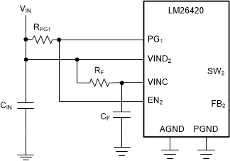
With Resistor DividerIf having a resistor divider to control VOUT2 with VOUT1 is not desired, then the PG1 can be connected to the EN2 pin to control VOUT2, see Figure 7-4. RPG1 is a pullup resistor on the range of 10 kΩ to 100 kΩ. 50 kΩ is the suggested value. This turns on VOUT2 when VOUT1 is approximately 85% of the programmed output.
Using PG1 to control VOUT2 also turns off VOUT2 when VOUT1 is outside the of the programmed output.
 Figure 7-4 PG1 Controlling
VOUT2
Figure 7-4 PG1 Controlling
VOUT2Another example is that the output is not to be turned on until the input voltage reaches 90% of desired voltage setpoint. This verifies that the input supply is stable before turning on the output. Select REN1 and REN2 so that the voltage at the EN pin is greater than 1.12 V when reaching the 90% desired set-point.
 Figure 7-5 Vin Controlling
VOUT
Figure 7-5 Vin Controlling
VOUTThe power-good feature of the LM26420-Q1 is designed with hysteresis to make sure no false power-good flags are asserted during large transient. After power good is asserted high, power good is not pulled low until the output voltage exceeds ±15% of the setpoint for a during of approximately 7.5 µs (typical), see Figure 7-6.
 Figure 7-6 Power-Good Hysteresis
Operation