JAJS559L September 1998 – June 2016 LM2671
PRODUCTION DATA.
- 1 特長
- 2 アプリケーション
- 3 概要
- 4 改訂履歴
- 5 Description (continued)
- 6 Pin Configuration and Functions
-
7 Specifications
- 7.1 Absolute Maximum Ratings
- 7.2 ESD Ratings
- 7.3 Recommended Operating Conditions
- 7.4 Thermal Information
- 7.5 Electrical Characteristics - 3.3 V
- 7.6 Electrical Characteristics - 5 V
- 7.7 Electrical Characteristics - 12 V
- 7.8 Electrical Characteristics - Adjustable
- 7.9 Electrical Characteristics - All Output Voltage Versions
- 7.10 Typical Characteristics
- 8 Detailed Description
-
9 Application and Implementation
- 9.1 Application Information
- 9.2 Typical Applications
- 10Power Supply Recommendations
- 11Layout
- 12デバイスおよびドキュメントのサポート
- 13メカニカル、パッケージ、および注文情報
パッケージ・オプション
メカニカル・データ(パッケージ|ピン)
サーマルパッド・メカニカル・データ
発注情報
9 Application and Implementation
NOTE
Information in the following applications sections is not part of the TI component specification, and TI does not warrant its accuracy or completeness. TI’s customers are responsible for determining suitability of components for their purposes. Customers should validate and test their design implementation to confirm system functionality.
9.1 Application Information
The LM2671 is a step-down DC-DC regulator. The device is typically used to convert a higher DC voltage to a lower DC voltage with a maximum output current of 0.5 A. The following design procedure can be used to select components for the LM2671. Alternately, the WEBENCH® software may be used to generate complete designs. When generating a design, the WEBENCH software uses iterative design procedure and accesses comprehensive databases of components. See ti.com for more details.
When the output voltage is greater than approximately 6 V, and the duty cycle at minimum input voltage is greater than approximately 50%, the designer must exercise caution in selection of the output filter components. When an application designed to these specific operating conditions is subjected to a current limit fault condition, it may be possible to observe a large hysteresis in the current limit. This can affect the output voltage of the device until the load current is reduced sufficiently to allow the current limit protection circuit to reset itself.
Under current limiting conditions, the LM267x is designed to respond in the following manner:
- At the moment when the inductor current reaches the current limit threshold, the ON-pulse is immediately terminated. This happens for any application condition.
- However, the current limit block is also designed to momentarily reduce the duty cycle to below 50% to avoid subharmonic oscillations, which could cause the inductor to saturate.
- Therefore, once the inductor current falls below the current limit threshold, there is a small relaxation time during which the duty cycle progressively rises back above 50% to the value required to achieve regulation.
If the output capacitance is sufficiently large, it might be possible that as the output tries to recover, the output capacitor charging current is large enough to repeatedly re-trigger the current limit circuit before the output has fully settled. This condition is exacerbated with higher output voltage settings because the energy requirement of the output capacitor varies as the square of the output voltage (½ CV2), thus requiring an increased charging current. A simple test to determine if this condition might exist for a suspect application is to apply a short circuit across the output of the converter, and then remove the shorted output condition. In an application with properly selected external components, the output recovers smoothly. Practical values of external components that have been experimentally found to work well under these specific operating conditions are COUT = 47 µF, L = 22 µH.
NOTE
Even with these components, for a device’s current limit of ICLIM, the maximum load current under which the possibility of the large current limit hysteresis can be minimized is ICLIM/2.
For example, if the input is 24 V and the set output voltage is 18 V, then for a desired maximum current of 1.5 A, the current limit of the chosen switcher must be confirmed to be at least 3 A. Under extreme overcurrent or short-circuit conditions, the LM267X employs frequency foldback in addition to the current limit. If the cycle-by-cycle inductor current increases above the current limit threshold (due to short circuit or inductor saturation for example) the switching frequency is automatically reduced to protect the IC. Frequency below 100 kHz is typical for an extreme short-circuit condition.
9.2 Typical Applications
9.2.1 Fixed Output Voltage Version
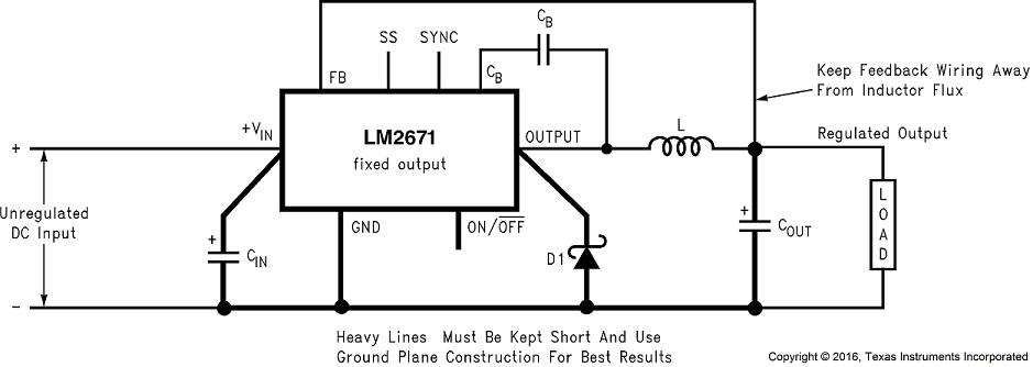
COUT = 47-μF, 25-V Tantalum, Sprague 595D Series
D1 = 3.3-A, 50-V Schottky Rectifier, IR 30WQ05F
L1 = 68-μH Sumida #RCR110D-680L
CB = 0.01-μF, 50-V ceramic
9.2.1.1 Design Requirements
Table 1 lists the design parameters for this example.
Table 1. Design Parameters
| PARAMETER | VALUE |
|---|---|
| Regulated output voltage (3.3 V, 5 V, or 12 V), VOUT | 5 V |
| Maximum DC input voltage, VIN(max) | 12 V |
| Maximum load current, ILOAD(max) | 500 mA |
9.2.1.2 Detailed Design Procedure
9.2.1.2.1 Inductor Selection (L1)
- Select the correct inductor value selection guide from Figure 17 and Figure 18 or Figure 19 (output voltages of 3.3 V, 5 V, or 12 V respectively). For all other voltages, see the design procedure for the adjustable version. Use the inductor selection guide for the 5-V version shown in Figure 18.
- From the inductor value selection guide, identify the inductance region intersected by the maximum input voltage line and the maximum load current line. Each region is identified by an inductance value and an inductor code (LXX). From the inductor value selection guide shown in Figure 18, the inductance region intersected by the 12-V horizontal line and the 500-mA vertical line is 47 μH, and the inductor code is L13.
- Select an appropriate inductor from the four manufacturer's part numbers listed in Table 2. Each manufacturer makes a different style of inductor to allow flexibility in meeting various design requirements. See the following for some of the differentiating characteristics of each manufacturer's inductors:
- Schottky: ferrite EP core inductors; these have very low leakage magnetic fields to reduce electro-magnetic interference (EMI) and are the lowest power loss inductors
- Renco: ferrite stick core inductors; benefits are typically lowest cost inductors and can withstand E•T and transient peak currents above rated value. Be aware that these inductors have an external magnetic field which may generate more EMI than other types of inductors.
- Pulse: powered iron toroid core inductors; these can also be low cost and can withstand larger than normal E•T and transient peak currents. Toroid inductors have low EMI.
- Coilcraft: ferrite drum core inductors; these are the smallest physical size inductors, available only as SMT components. Be aware that these inductors also generate EMI—but less than stick inductors.
Complete specifications for these inductors are available from the respective manufacturers.
The inductance value required is 47 μH. From the table in Table 2, go to the L13 line and choose an inductor part number from any of the four manufacturers shown. In most instances, both through hole and surface mount inductors are available.
Table 2. Inductor Manufacturers' Part Numbers
| IND. REF. DESG. |
INDUCTANCE (μH) |
CURRENT (A) |
SCHOTTKY | RENCO | PULSE ENGINEERING | COILCRAFT | |||
|---|---|---|---|---|---|---|---|---|---|
| THROUGH HOLE | SURFACE MOUNT | THROUGH HOLE | SURFACE MOUNT | THROUGH HOLE | SURFACE MOUNT | SURFACE MOUNT | |||
| L2 | 150 | 0.21 | 67143920 | 67144290 | RL-5470-4 | RL1500-150 | PE-53802 | PE-53802-S | DO1608-154 |
| L3 | 100 | 0.26 | 67143930 | 67144300 | RL-5470-5 | RL1500-100 | PE-53803 | PE-53803-S | DO1608-104 |
| L4 | 68 | 0.32 | 67143940 | 67144310 | RL-1284-68-43 | RL1500-68 | PE-53804 | PE-53804-S | DO1608-683 |
| L5 | 47 | 0.37 | 67148310 | 67148420 | RL-1284-47-43 | RL1500-47 | PE-53805 | PE-53805-S | DO1608-473 |
| L6 | 33 | 0.44 | 67148320 | 67148430 | RL-1284-33-43 | RL1500-33 | PE-53806 | PE-53806-S | DO1608-333 |
| L7 | 22 | 0.52 | 67148330 | 67148440 | RL-1284-22-43 | RL1500-22 | PE-53807 | PE-53807-S | DO1608-223 |
| L9 | 220 | 0.32 | 67143960 | 67144330 | RL-5470-3 | RL1500-220 | PE-53809 | PE-53809-S | DO3308-224 |
| L10 | 150 | 0.39 | 67143970 | 67144340 | RL-5470-4 | RL1500-150 | PE-53810 | PE-53810-S | DO3308-154 |
| L11 | 100 | 0.48 | 67143980 | 67144350 | RL-5470-5 | RL1500-100 | PE-53811 | PE-53811-S | DO3308-104 |
| L12 | 68 | 0.58 | 67143990 | 67144360 | RL-5470-6 | RL1500-68 | PE-53812 | PE-53812-S | DO3308-683 |
| L13 | 47 | 0.7 | 67144000 | 67144380 | RL-5470-7 | RL1500-47 | PE-53813 | PE-53813-S | DO3308-473 |
| L14 | 33 | 0.83 | 67148340 | 67148450 | RL-1284-33-43 | RL1500-33 | PE-53814 | PE-53814-S | DO3308-333 |
| L15 | 22 | 0.99 | 67148350 | 67148460 | RL-1284-22-43 | RL1500-22 | PE-53815 | PE-53815-S | DO3308-223 |
| L18 | 220 | 0.55 | 67144040 | 67144420 | RL-5471-2 | RL1500-220 | PE-53818 | PE-53818-S | DO3316-224 |
| L19 | 150 | 0.66 | 67144050 | 67144430 | RL-5471-3 | RL1500-150 | PE-53819 | PE-53819-S | DO3316-154 |
| L20 | 100 | 0.82 | 67144060 | 67144440 | RL-5471-4 | RL1500-100 | PE-53820 | PE-53820-S | DO3316-104 |
| L21 | 68 | 0.99 | 67144070 | 67144450 | RL-5471-5 | RL1500-68 | PE-53821 | PE-53821-S | DO3316-683 |
9.2.1.2.2 Output Capacitor Selection (COUT)
Select an output capacitor from the output capacitor table in Table 9. Using the output voltage and the inductance value found in the inductor selection guide, step 1, locate the appropriate capacitor value and voltage rating.
Use the 5-V section in the output capacitor table in Table 9. Choose a capacitor value and voltage rating from the line that contains the inductance value of 47 μH. The capacitance and voltage rating values corresponding to the 47-μH inductor are:
- Surface mount:
- 68-μF, 10-V Sprague 594D series
- 100-μF, 10-V AVX TPS series
- Through hole:
- 68-μF, 10-V Sanyo OS-CON SA series
- 150-μF, 35-V Sanyo MV-GX series
- 150-μF, 35-V Nichicon PL series
- 150-μF, 35-V Panasonic HFQ series
The capacitor list contains through-hole electrolytic capacitors from four different capacitor manufacturers and surface mount tantalum capacitors from two different capacitor manufacturers. TI recommends that both the manufacturers and the manufacturer's series that are listed in the table be used.
Table 3. Output Capacitor Table
| OUTPUT VOLTAGE (V) |
INDUCTANCE (μH) |
OUTPUT CAPACITOR | |||||
|---|---|---|---|---|---|---|---|
| SURFACE MOUNT | THROUGH HOLE | ||||||
| SPRAGUE 594D SERIES (μF/V) | AVX TPS SERIES (μF/V) | SANYO OS-CON SA SERIES (μF/V) | SANYO MV-GX SERIES (μF/V) | NICHICON PL SERIES (μF/V) | PANASONIC HFQ SERIES (μF/V) | ||
| 3.3 | 22 | 120/6.3 | 100/10 | 100/10 | 330/35 | 330/35 | 330/35 |
| 33 | 120/6.3 | 100/10 | 68/10 | 220/35 | 220/35 | 220/35 | |
| 47 | 68/10 | 100/10 | 68/10 | 150/35 | 150/35 | 150/35 | |
| 68 | 120/6.3 | 100/10 | 100/10 | 120/35 | 120/35 | 120/35 | |
| 100 | 120/6.3 | 100/10 | 100/10 | 120/35 | 120/35 | 120/35 | |
| 150 | 120/6.3 | 100/10 | 100/10 | 120/35 | 120/35 | 120/35 | |
| 5 | 22 | 100/16 | 100/10 | 100/10 | 330/35 | 330/35 | 330/35 |
| 33 | 68/10 | 10010 | 68/10 | 220/35 | 220/35 | 220/35 | |
| 47 | 68/10 | 100/10 | 68/10 | 150/35 | 150/35 | 150/35 | |
| 68 | 100/16 | 100/10 | 100/10 | 120/35 | 120/35 | 120/35 | |
| 100 | 100/16 | 100/10 | 100/10 | 120/35 | 120/35 | 120/35 | |
| 150 | 100/16 | 100/10 | 100/10 | 120/35 | 120/35 | 120/35 | |
| 12 | 22 | 120/20 | (2×) 68/20 | 68/20 | 330/35 | 330/35 | 330/35 |
| 33 | 68/25 | 68/20 | 68/20 | 220/35 | 220/35 | 220/35 | |
| 47 | 47/20 | 68/20 | 47/20 | 150/35 | 150/35 | 150/35 | |
| 68 | 47/20 | 68/20 | 47/20 | 120/35 | 120/35 | 120/35 | |
| 100 | 47/20 | 68/20 | 47/20 | 120/35 | 120/35 | 120/35 | |
| 150 | 47/20 | 68/20 | 47/20 | 120/35 | 120/35 | 120/35 | |
| 220 | 47/20 | 68/20 | 47/20 | 120/35 | 120/35 | 120/35 | |
9.2.1.2.3 Catch Diode Selection (D1)
- In normal operation, the average current of the catch diode is the load current times the catch diode duty cycle, 1-D (D is the switch duty cycle, which is approximately the output voltage divided by the input voltage). The largest value of the catch diode average current occurs at the maximum load current and maximum input voltage (minimum D). For normal operation, the catch diode current rating must be at least 1.3 times greater than its maximum average current. However, if the power supply design must withstand a continuous output short, the diode must have a current rating equal to the maximum current limit of the LM2671. The most stressful condition for this diode is a shorted output condition (refer to Table 4). In this example, a 1-A, 20-V Schottky diode provides the best performance. If the circuit must withstand a continuous shorted output, TI recommends a higher-current Schottky diode.
- The reverse voltage rating of the diode must be at least 1.25 times the maximum input voltage.
- Because of their fast switching speed and low forward voltage drop, Schottky diodes provide the best performance and efficiency. This Schottky diode must be placed close to the LM2671 using short leads and short printed-circuit traces.
Table 4. Schottky Diode Selection Table
| VR | 1-A DIODES | 3-A DIODES | ||
|---|---|---|---|---|
| SURFACE MOUNT | THROUGH HOLE | SURFACE MOUNT | THROUGH HOLE | |
| 20 V | SK12 | 1N5817 | SK32 | 1N5820 |
| B120 | SR102 | — | SR302 | |
| 30 V | SK13 | 1N5818 | SK33 | 1N5821 |
| B130 | 11DQ03 | 30WQ03F | 31DQ03 | |
| MBRS130 | SR103 | — | — | |
| 40 V | SK14 | 1N5819 | SK34 | 1N5822 |
| B140 | 11DQ04 | 30BQ040 | MBR340 | |
| MBRS140 | SR104 | 30WQ04F | 31DQ04 | |
| 10BQ040 | — | MBRS340 | SR304 | |
| 10MQ040 | — | MBRD340 | — | |
| 15MQ040 | — | — | — | |
| 50 V | SK15 | MBR150 | SK35 | MBR350 |
| B150 | 11DQ05 | 30WQ05F | 31DQ05 | |
| 10BQ050 | SR105 | — | SR305 | |
9.2.1.2.4 Input Capacitor (CIN)
A low ESR aluminum or tantalum bypass capacitor is required between the input pin and ground to prevent large voltage transients from appearing at the input. This capacitor must be placed close to the IC using short leads. In addition, the RMS current rating of the input capacitor must be selected to be at least ½ the DC load current. The capacitor manufacturer data sheet must be checked to assure that this current rating is not exceeded. The curves shown in Figure 16 show typical RMS current ratings for several different aluminum electrolytic capacitor values. A parallel connection of two or more capacitors may be required to increase the total minimum RMS current rating to suit the application requirements.
For an aluminum electrolytic capacitor, the voltage rating must be at least 1.25 times the maximum input voltage. Caution must be exercised if solid tantalum capacitors are used. The tantalum capacitor voltage rating must be twice the maximum input voltage. Table 5 and Table 6 show the recommended application voltage for AVX TPS and Sprague 594D tantalum capacitors. TI also recommends that they be surge current tested by the manufacturer. The TPS series available from AVX, and the 593D and 594D series from Sprague are all surge current tested. Another approach to minimize the surge current stresses on the input capacitor is to add a small inductor in series with the input supply line.
Table 5. AVX TPS
| RECOMMENDED APPLICATION VOLTAGE |
VOLTAGE RATING |
|---|---|
| 85°C RATING | |
| 3.3 | 6.3 |
| 5 | 10 |
| 10 | 20 |
| 12 | 25 |
| 15 | 35 |
Table 6. Sprague 594D
| RECOMMENDED APPLICATION VOLTAGE |
VOLTAGE RATING |
|---|---|
| 85°C RATING | |
| 2.5 | 4 |
| 3.3 | 6.3 |
| 5 | 10 |
| 8 | 16 |
| 12 | 20 |
| 18 | 25 |
| 24 | 35 |
| 29 | 50 |
Use caution when using ceramic capacitors for input bypassing, because it may cause severe ringing at the VIN pin. The important parameters for the input capacitor are the input voltage rating and the RMS current rating. With a maximum input voltage of 12 V, an aluminum electrolytic capacitor with a voltage rating greater than 15 V (1.25 × VIN) is required. The next higher capacitor voltage rating is 16 V.
The RMS current rating requirement for the input capacitor in a buck regulator is approximately ½ the DC load current. In this example, with a 500-mA load, a capacitor with a RMS current rating of at least 250 mA is required. The curves shown in Figure 16 can be used to select an appropriate input capacitor. From the curves, locate the 16-V line and note which capacitor values have RMS current ratings greater than 250 mA.
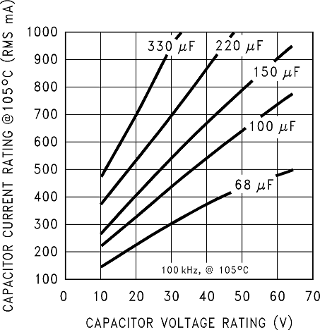 Figure 16. RMS Current Ratings for Low ESR Electrolytic Capacitors (Typical)
For a through-hole design, a 100-μF, 16-V electrolytic capacitor (Panasonic HFQ series, Nichicon PL, Sanyo MV-GX series or equivalent) would be adequate. Other types or other manufacturers' capacitors can be used provided the RMS ripple current ratings are adequate. Additionally, for a complete surface mount design, electrolytic capacitors such as the Sanyo CV-C or CV-BS and the Nichicon WF or UR and the NIC Components NACZ series could be considered.
For surface mount designs, solid tantalum capacitors can be used, but caution must be exercised with regard to the capacitor surge current rating and voltage rating. In this example, checking the Sprague 594D series datasheet, a Sprague 594D 15-μF, 25-V capacitor is adequate.
9.2.1.2.5 Boost Capacitor (CB)
This capacitor develops the necessary voltage to turn the switch gate on fully. All applications must use a
0.01-μF, 50-V ceramic capacitor. For this application, and all applications, use a 0.01-μF, 50-V ceramic capacitor.
9.2.1.2.6 Soft-Start Capacitor (CSS) – Optional
This capacitor controls the rate at which the device starts up. The formula for the soft-start capacitor CSS is Equation 1.

where
- ISS= soft-start current (4.5 μA typical)
- tSS= soft-start time (selected)
- VSSTH= soft-start threshold voltage (0.63 V typical)
- VOUT= output voltage (selected)
- VSCHOTTKY= schottky diode voltage drop (0.4 V typical)
- VIN= input voltage (selected)
For this application, selecting a start-up time of 10 ms and using Equation 2 for CSS.

If this feature is not desired, leave this pin open. With certain soft-start capacitor values and operating conditions, the LM2671 can exhibit an overshoot on the output voltage during turnon. Especially when starting up into no load or low load, the soft-start function may not be effective in preventing a larger voltage overshoot on the output. With larger loads or lower input voltages during start-up this effect is minimized. In particular, avoid using soft-start capacitors between 0.033 µF and 1 µF.
9.2.1.2.7 Frequency Synchronization (optional)
The LM2671 (oscillator) can be synchronized to run with an external oscillator, using the sync pin (pin 3). By doing so, the LM2671 can be operated at higher frequencies than the standard frequency of 260 kHz. This allows for a reduction in the size of the inductor and output capacitor.
As shown in the drawing below, a signal applied to a RC filter at the sync pin causes the device to synchronize to the frequency of that signal. For a signal with a peak-to-peak amplitude of 3 V or greater, a 1-kΩ resistor and a 100-pF capacitor are suitable values.

For all applications, use a 1-kΩ resistor and a 100-pF capacitor for the RC filter.
9.2.1.3 Application Curves
for continuous mode operation
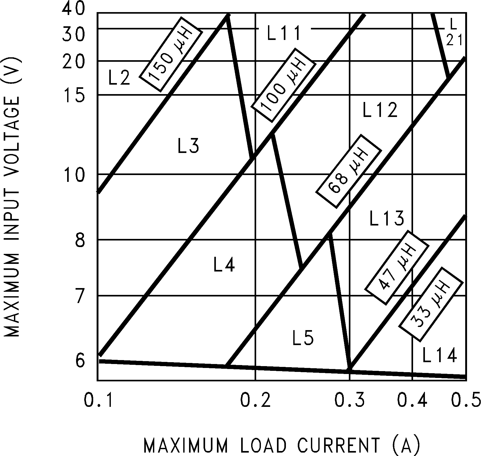 Figure 17. LM2671-3.3
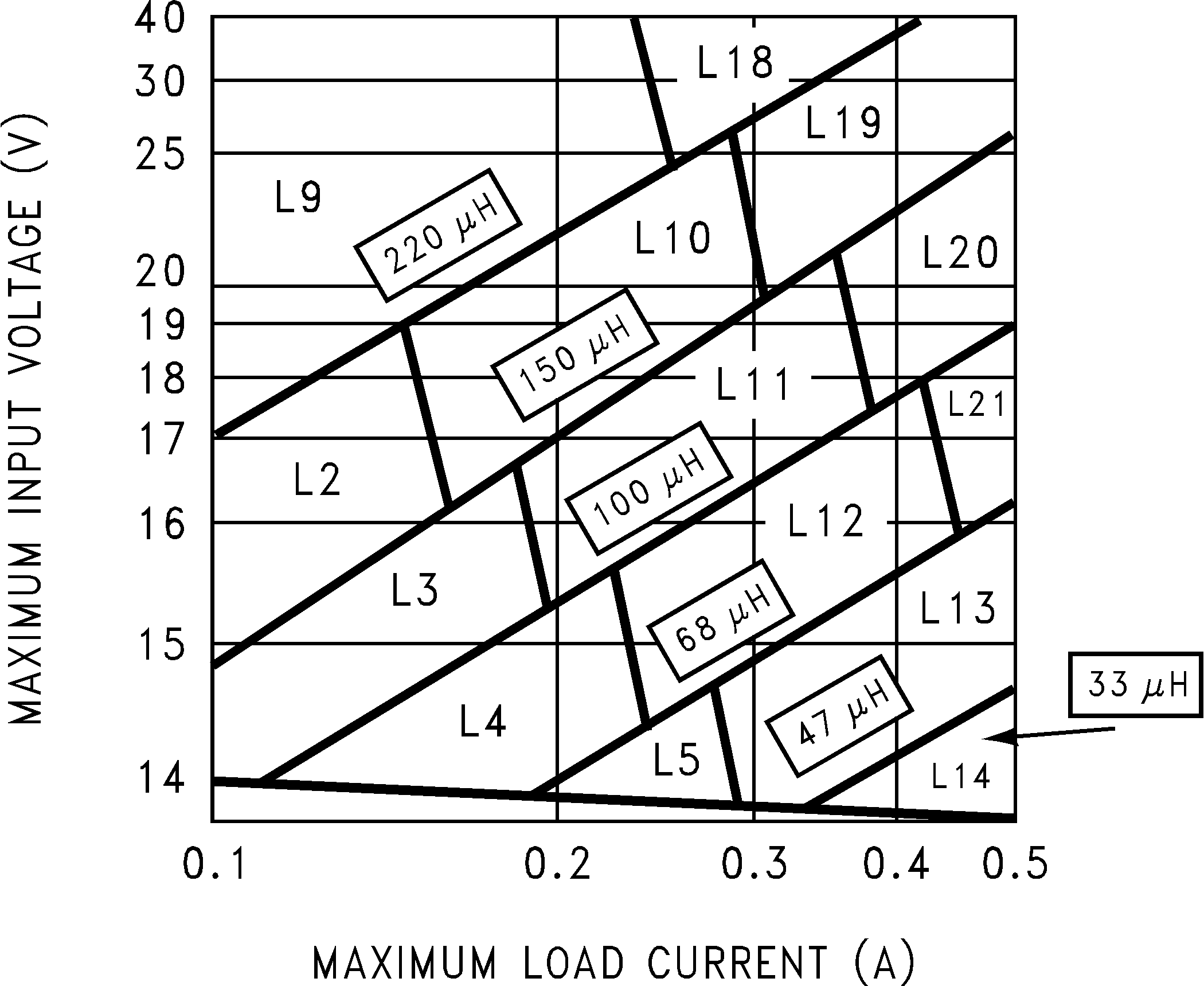 Figure 19. LM2671-12
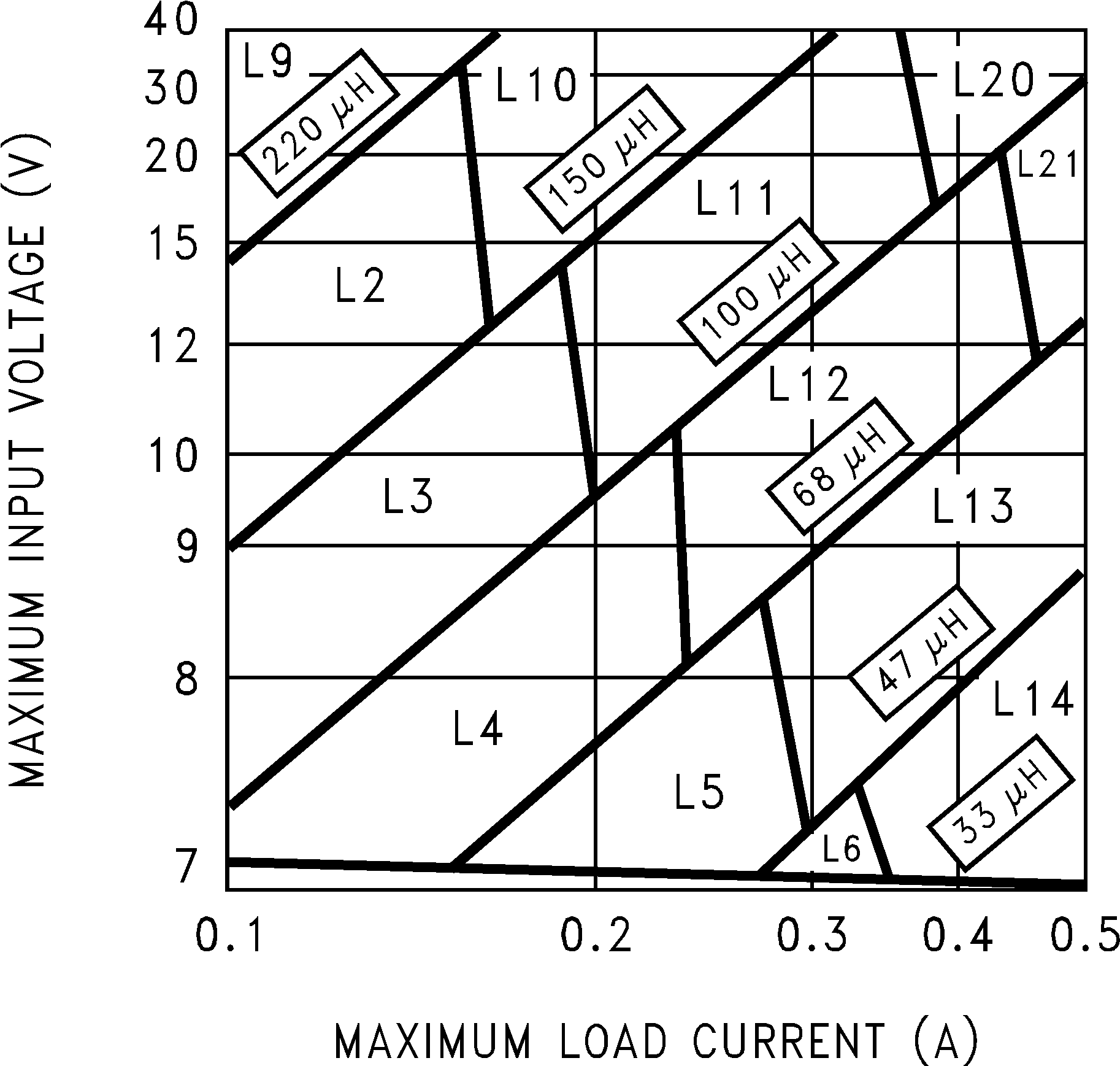 Figure 18. LM2671-5
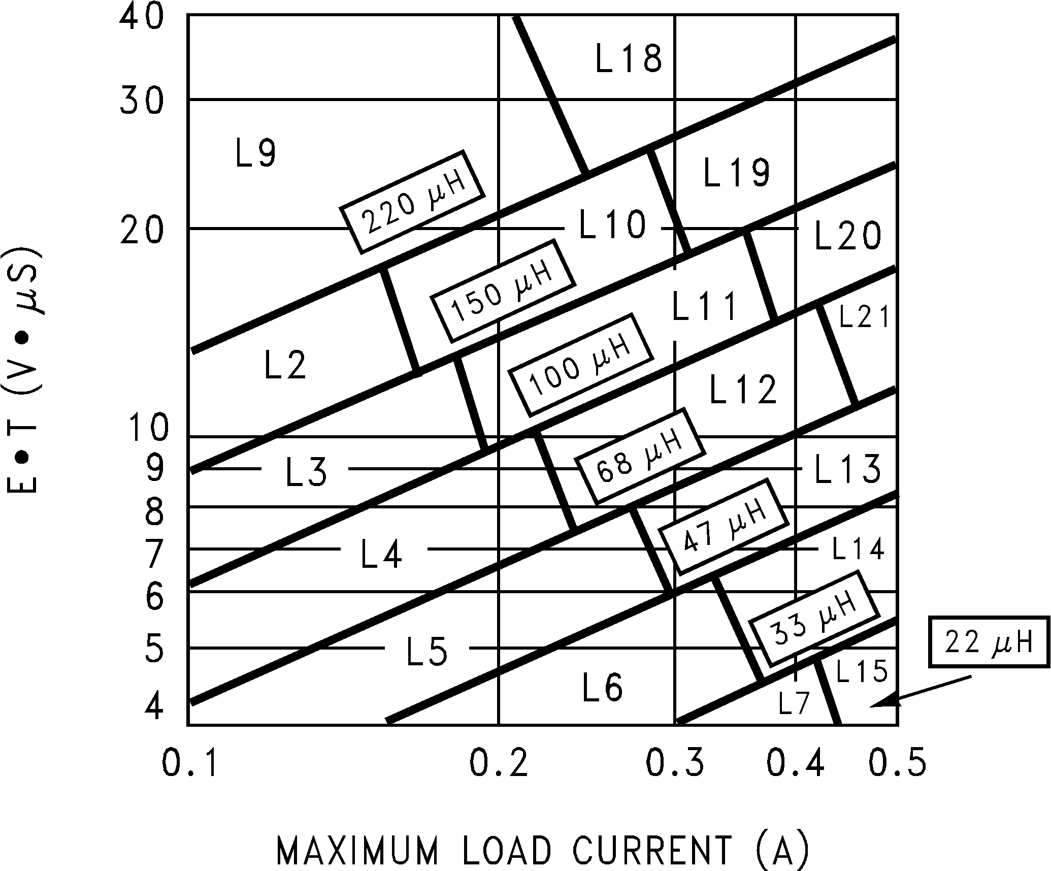 Figure 20. LM2671-ADJ
9.2.2 Adjustable Output Voltage Version
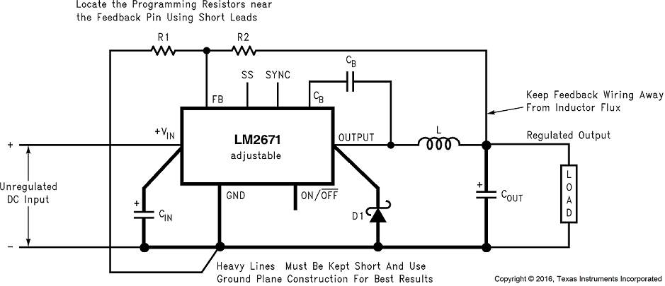
COUT = 47-μF, 25-V Tantalum, Sprague 595D Series
D1 = 3.3-A, 50-V Schottky Rectifier, IR 30WQ05F
L1 = 68-μH Sumida #RCR110D-680L
R1 =1.5 kΩ, 1%
CB = 0.01-μF, 50-V ceramic
9.2.2.1 Design Requirements
Table 7 lists the design parameters for this example.
Table 7. Design Parameters
| PARAMETER | VALUE |
|---|---|
| Regulated output voltage, VOUT | 20 V |
| Maximum input voltage, VIN(max) | 28 V |
| Maximum load current, ILOAD(max) | 500 mA |
| Switching frequency, F | Fixed at a nominal 260 kHz |
9.2.2.2 Detailed Design Procedure
9.2.2.2.1 Programming Output Voltage
Select R1 and R2, as shown in Figure 21.
Use the following formula to select the appropriate resistor values.

where
- VREF = 1.21 V
Select R1 to be 1 kΩ, 1%. Solve for R2.

Select a value for R1 between 240 Ω and 1.5 kΩ. The lower resistor values minimize noise pickup in the sensitive feedback pin. For the lowest temperature coefficient and the best stability with time, use 1% metal film resistors.

R2 = 1 kΩ (16.53 − 1) = 15.53 kΩ, closest 1% value is 15.4 kΩ.
R2 = 15.4 kΩ.
9.2.2.2.2 Inductor Selection (L1)
- Calculate the inductor Volt • microsecond constant E • T (V • μs) from Equation 6.
- VSAT = internal switch saturation voltage = 0.25 V
- VD = diode forward voltage drop = 0.5 V
- Use the E • T value from the previous formula and match it with the E • T number on the vertical axis of the inductor value selection guide shown in Figure 20.
- On the horizontal axis, select the maximum load current in Equation 9.
- Identify the inductance region intersected by the E • T value and the maximum load current value. Each region is identified by an inductance value and an inductor code (LXX). From the inductor value selection guide shown in Figure 20, the inductance region intersected by the 21.6 (V • μs) horizontal line and the 500-mA vertical line is 100 μH, and the inductor code is L20.
- Select an appropriate inductor from the four manufacturer's part numbers listed in Table 2. For information on the different types of inductors, see the inductor selection in the fixed output voltage design procedure. From the table in Table 2, locate line L20, and select an inductor part number from the list of manufacturers' part numbers.

where
Calculate the inductor Volt • microsecond constant (E • T) with Equation 7.

9.2.2.2.3 Output Capacitor Selection (COUT)
- Select an output capacitor from the capacitor code selection guide in Table 8. Using the inductance value found in the inductor selection guide, step 1, locate the appropriate capacitor code corresponding to the desired output voltage. Use the appropriate row of the capacitor code selection guide, in Table 8. For this example, use the 15-V to 20-V row. The capacitor code corresponding to an inductance of 100 μH is C20.
- Select an appropriate capacitor value and voltage rating, using the capacitor code, from the output capacitor selection table in Table 9. There are two solid tantalum (surface mount) capacitor manufacturers and four electrolytic (through hole) capacitor manufacturers to choose from. TI recommends using the manufacturers and the manufacturer's series that are listed in the table.
- Surface mount:
- 33-μF, 25-V Sprague 594D series
- 33-μF, 25-V AVX TPS series
- Through hole:
- 33-μF, 25-V Sanyo OS-CON SC series
- 120-μF, 35-V Sanyo MV-GX series
- 120-μF, 35-V Nichicon PL series
- 120-μF, 35-V Panasonic HFQ series
From the output capacitor selection table in Table 9, choose a capacitor value (and voltage rating) that intersects the capacitor code(s) selected in section A, C20.
The capacitance and voltage rating values corresponding to the capacitor code C20 are:
Other manufacturers or other types of capacitors may also be used, provided the capacitor specifications (especially the 100-kHz ESR) closely match the characteristics of the capacitors listed in the output capacitor table. See the capacitor manufacturers' data sheet for this information.
Table 8. Capacitor Code Selection Guide
| CASE STYLE (1) |
OUTPUT VOLTAGE (V) |
INDUCTANCE (μH) | ||||||
|---|---|---|---|---|---|---|---|---|
| 22 | 33 | 47 | 68 | 100 | 150 | 220 | ||
| SM and TH | 1.21–2.5 | — | — | — | — | C1 | C2 | C3 |
| SM and TH | 2.5–3.75 | — | — | — | C1 | C2 | C3 | C3 |
| SM and TH | 3.75–5 | — | — | C4 | C5 | C6 | C6 | C6 |
| SM and TH | 5–6.25 | — | C4 | C7 | C6 | C6 | C6 | C6 |
| SM and TH | 6.25–7.5 | C8 | C4 | C7 | C6 | C6 | C6 | C6 |
| SM and TH | 7.5–10 | C9 | C10 | C11 | C12 | C13 | C13 | C13 |
| SM and TH | 10–12.5 | C14 | C11 | C12 | C12 | C13 | C13 | C13 |
| SM and TH | 12.5–15 | C15 | C16 | C17 | C17 | C17 | C17 | C17 |
| SM and TH | 15–20 | C18 | C19 | C20 | C20 | C20 | C20 | C20 |
| SM and TH | 20–30 | C21 | C22 | C22 | C22 | C22 | C22 | C22 |
| TH | 30–37 | C23 | C24 | C24 | C25 | C25 | C25 | C25 |
Table 9. Output Capacitor Selection Table
| OUTPUT CAPACITOR | ||||||
|---|---|---|---|---|---|---|
| CAP. REF. DESG. # |
SURFACE MOUNT | THROUGH HOLE | ||||
| SPRAGUE 594D SERIES (μF/V) | AVX TPS SERIES (μF/V) | SANYO OS-CON SA SERIES (μF/V) | SANYO MV-GX SERIES (μF/V) | NICHICON PL SERIES (μF/V) | PANASONIC HFQ SERIES (μF/V) | |
| C1 | 120/6.3 | 100/10 | 100/10 | 220/35 | 220/35 | 220/35 |
| C2 | 120/6.3 | 100/10 | 100/10 | 150/35 | 150/35 | 150/35 |
| C3 | 120/6.3 | 100/10 | 100/35 | 120/35 | 120/35 | 120/35 |
| C4 | 68/10 | 100/10 | 68/10 | 220/35 | 220/35 | 220/35 |
| C5 | 100/16 | 100/10 | 100/10 | 150/35 | 150/35 | 150/35 |
| C6 | 100/16 | 100/10 | 100/10 | 120/35 | 120/35 | 120/35 |
| C7 | 68/10 | 100/10 | 68/10 | 150/35 | 150/35 | 150/35 |
| C8 | 100/16 | 100/10 | 100/10 | 330/35 | 330/35 | 330/35 |
| C9 | 100/16 | 100/16 | 100/16 | 330/35 | 330/35 | 330/35 |
| C10 | 100/16 | 100/16 | 68/16 | 220/35 | 220/35 | 220/35 |
| C11 | 100/16 | 100/16 | 68/16 | 150/35 | 150/35 | 150/35 |
| C12 | 100/16 | 100/16 | 68/16 | 120/35 | 120/35 | 120/35 |
| C13 | 100/16 | 100/16 | 100/16 | 120/35 | 120/35 | 120/35 |
| C14 | 100/16 | 100/16 | 100/16 | 220/35 | 220/35 | 220/35 |
| C15 | 47/20 | 68/20 | 47/20 | 220/35 | 220/35 | 220/35 |
| C16 | 47/20 | 68/20 | 47/20 | 150/35 | 150/35 | 150/35 |
| C17 | 47/20 | 68/20 | 47/20 | 120/35 | 120/35 | 120/35 |
| C18 | 68/25 | (2×) 33/25 | 47/25 (1) | 220/35 | 220/35 | 220/35 |
| C19 | 33/25 | 33/25 | 33/25 (1) | 150/35 | 150/35 | 150/35 |
| C20 | 33/25 | 33/25 | 33/25 (1) | 120/35 | 120/35 | 120/35 |
| C21 | 33/35 | (2×) 22/25 | (2) | 150/35 | 150/35 | 150/35 |
| C22 | 33/35 | 22/35 | (2) | 120/35 | 120/35 | 120/35 |
| C23 | (2) | (2) | (2) | 220/50 | 100/50 | 120/50 |
| C24 | (2) | (2) | (2) | 150/50 | 100/50 | 120/50 |
| C25 | (2) | (2) | (2) | 150/50 | 82/50 | 82/50 |
9.2.2.2.4 Catch Diode Selection (D1)
- In normal operation, the average current of the catch diode is the load current times the catch diode duty cycle, 1-D (D is the switch duty cycle, which is approximately VOUT/VIN). The largest value of the catch diode average current occurs at the maximum input voltage (minimum D). For normal operation, the catch diode current rating must be at least 1.3 times greater than its maximum average current. However, if the power supply design must withstand a continuous output short, the diode must have a current rating greater than the maximum current limit of the LM2671. The most stressful condition for this diode is a shorted output condition.
- The reverse voltage rating of the diode must be at least 1.25 times the maximum input voltage.
- Because of their fast switching speed and low forward voltage drop, Schottky diodes provide the best performance and efficiency. The Schottky diode must be placed close to the LM2671 using short leads and short printed-circuit traces.
Refer to the table shown in Table 4. Schottky diodes provide the best performance, and in this example a 1-A, 40-V Schottky diode would be a good choice. If the circuit must withstand a continuous shorted output, a higher current (at least 1.2 A) Schottky diode is recommended.
9.2.2.2.5 Input Capacitor (CIN)
A low ESR aluminum or tantalum bypass capacitor is required between the input pin and ground to prevent large voltage transients from appearing at the input. This capacitor must be placed close to the IC using short leads. In addition, the RMS current rating of the input capacitor must be selected to be at least ½ the DC load current. The capacitor manufacturer data sheet must be checked to assure that this current rating is not exceeded. The curves shown in Figure 16 show typical RMS current ratings for several different aluminum electrolytic capacitor values. A parallel connection of two or more capacitors may be required to increase the total minimum RMS current rating to suit the application requirements.
For an aluminum electrolytic capacitor, the voltage rating must be at least 1.25 times the maximum input voltage. Caution must be exercised if solid tantalum capacitors are used. The tantalum capacitor voltage rating must be twice the maximum input voltage. The Table 10 and Table 11 show the recommended application voltage for AVX TPS and Sprague 594D tantalum capacitors. TI also recommends that they be surge current tested by the manufacturer. The TPS series available from AVX, and the 593D and 594D series from Sprague are all surge current tested. Another approach to minimize the surge current stresses on the input capacitor is to add a small inductor in series with the input supply line.
Table 10. AVX TPS
| RECOMMENDED APPLICATION VOLTAGE |
VOLTAGE RATING |
|---|---|
| 85°C RATING | |
| 3.3 | 6.3 |
| 5 | 10 |
| 10 | 20 |
| 12 | 25 |
| 15 | 35 |
Table 11. Sprague 594D
| RECOMMENDED APPLICATION VOLTAGE |
VOLTAGE RATING |
|---|---|
| 85°C RATING | |
| 2.5 | 4 |
| 3.3 | 6.3 |
| 5 | 10 |
| 8 | 16 |
| 12 | 20 |
| 18 | 25 |
| 24 | 35 |
| 29 | 50 |
Use caution when using ceramic capacitors for input bypassing, because it may cause severe ringing at the VIN pin.
The important parameters for the input capacitor are the input voltage rating and the RMS current rating. With a maximum input voltage of 28 V, an aluminum electrolytic capacitor with a voltage rating of at least
35 V (1.25 × VIN) is required.
The RMS current rating requirement for the input capacitor in a buck regulator is approximately ½ the DC load current. In this example, with a 500-mA load, a capacitor with a RMS current rating of at least 250 mA is required. The curves shown in Figure 22 can be used to select an appropriate input capacitor. From the curves, locate the 35-V line and note which capacitor values have RMS current ratings greater than 250 mA.
 Figure 22. RMS Current Ratings for Low ESR Electrolytic Capacitors (Typical)
For a through-hole design, a 68-μF, 35-V electrolytic capacitor (Panasonic HFQ series, Nichicon PL, Sanyo MV-GX series or equivalent) would be adequate. Other types or other manufacturers' capacitors can be used provided the RMS ripple current ratings are adequate. Additionally, for a complete surface mount design, electrolytic capacitors such as the Sanyo CV-C or CV-BS and the Nichicon WF or UR and the NIC Components NACZ series could be considered.
For surface mount designs, solid tantalum capacitors can be used, but caution must be exercised with regard to the capacitor surge current rating and voltage rating. In this example, checking the Sprague 594D series data sheet, a Sprague 594D 15-μF, 50-V capacitor is adequate.
9.2.2.2.6 Boost Capacitor (CB)
This capacitor develops the necessary voltage to turn the switch gate on fully. All applications must use a
0.01-μF, 50-V ceramic capacitor. For this application, and all applications, use a 0.01-μF, 50-V ceramic capacitor.
If the soft-start and frequency synchronization features are desired, look at steps 6 and 7 in Detailed Design Procedure.
9.2.2.3 Application Curves
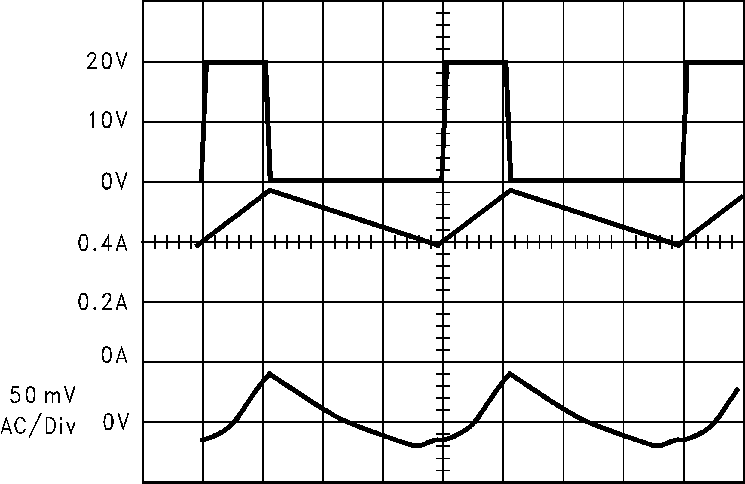
| Continuous Mode Switching Waveforms, VIN = 20 V, VOUT = 5 V, ILOAD = 500 mA, L = 100 μH, COUT = 100 μF, COUTESR = 0.1 Ω |
||
| A: VSW pin voltage, 10 V/div. | ||
| B: Inductor current, 0.2 A/div | ||
| C: Output ripple voltage, 50 mV/div ac-coupled | ||
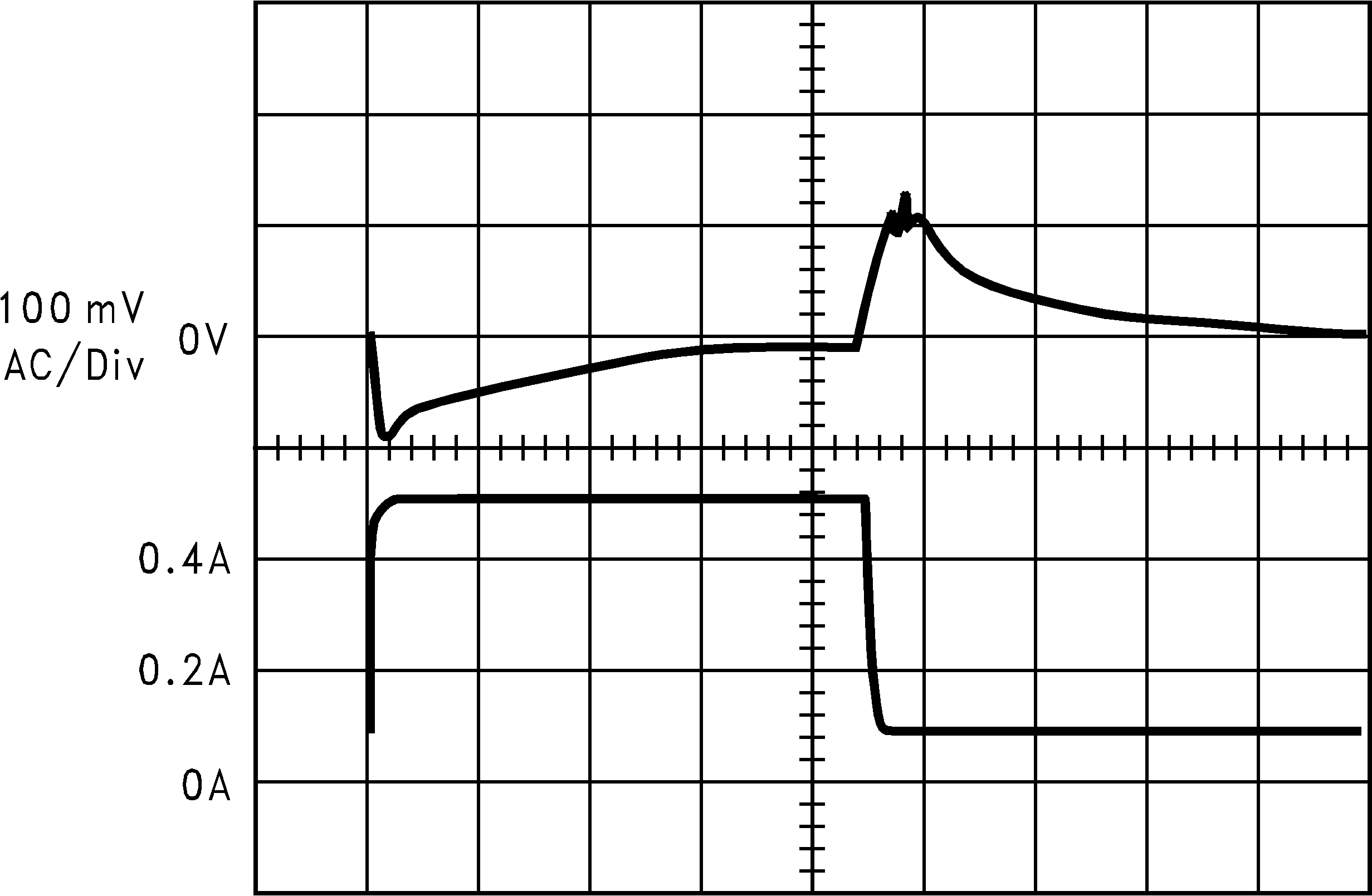
| Load Transient Response for Continuous Mode, VIN = 20 V, VOUT = 5 V, L = 100 μH, COUT = 100 μF, COUTESR = 0.1 Ω |
||
| A: Output voltage, 100 mV/div, ac-coupled | ||
| B: Load current: 100-mA to 500-mA load pulse |
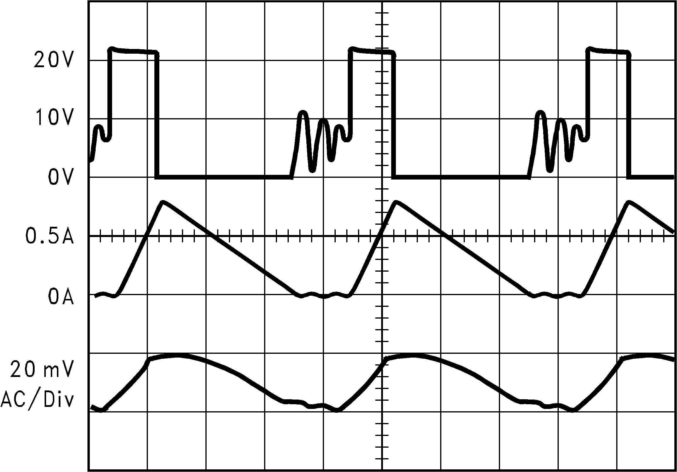
| Discontinuous Mode Switching Waveforms, VIN = 20 V, VOUT = 5 V, ILOAD = 300 mA, L = 15 μH, COUT = 68 μF (2×), COUTESR = 25 mΩ |
||
| A: VSW pin voltage, 10 V/div. | ||
| B: Inductor current, 0.5 A/div | ||
| C: Output ripple voltage, 20 mV/div ac-coupled |
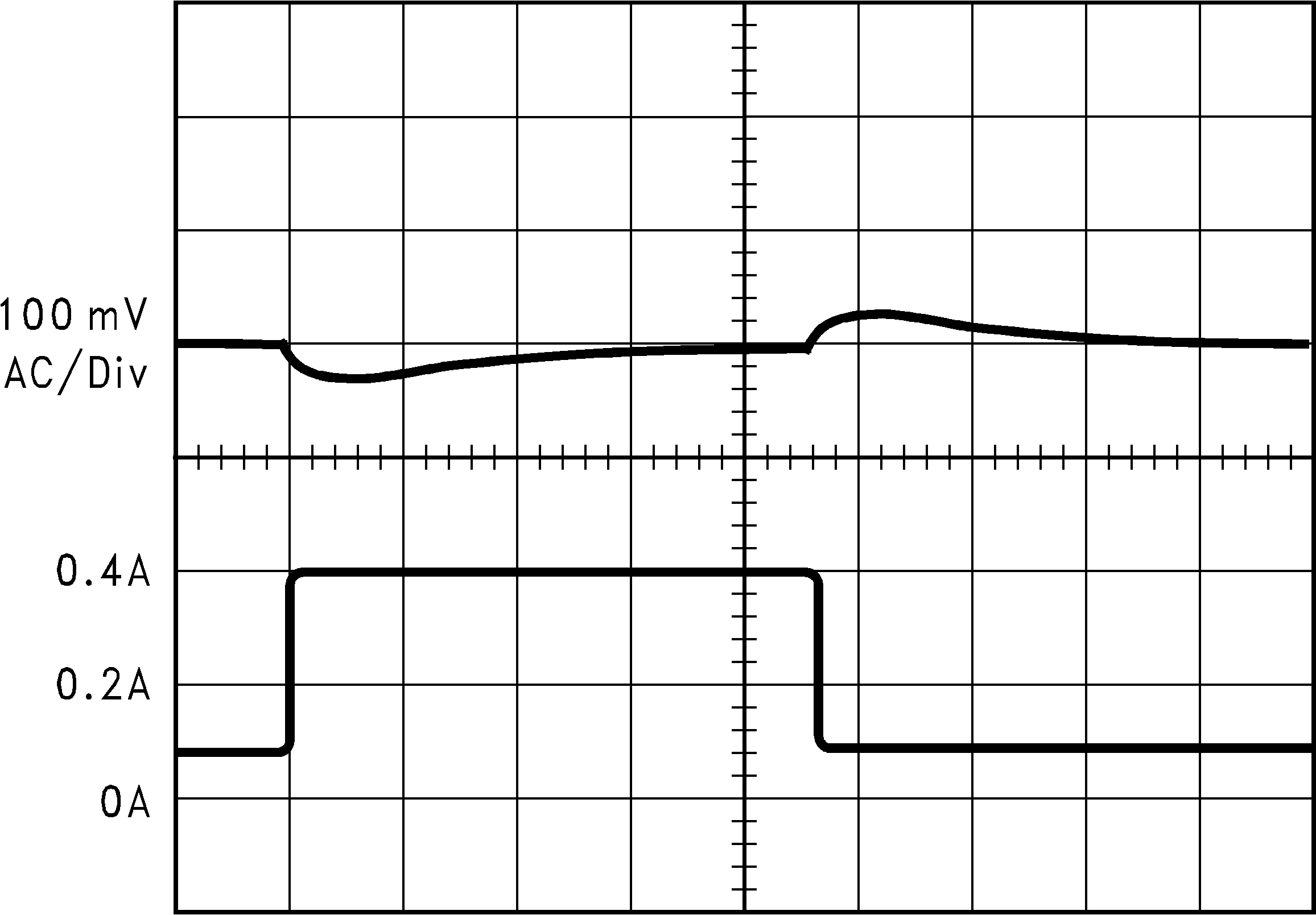
| Load Transient Response for Discontinuous Mode, VIN = 20 V, VOUT = 5 V, L = 47 μH, COUT = 68 μF, COUTESR = 50 mΩ |
||
| A: Output voltage, 100 mV/div, ac-coupled | ||
| B: Load current: 100-mA to 400-mA load pulse |