-
LM2673 SIMPLE SWITCHER®3A降圧型電圧レギュレータ、電流制限調整機能付き
- 1 特長
- 2 アプリケーション
- 3 概要
- 4 改訂履歴
- 5 Pin Configuration and Functions
-
6 Specifications
- 6.1 Absolute Maximum Ratings
- 6.2 ESD Ratings
- 6.3 Recommended Operating Conditions
- 6.4 Thermal Information
- 6.5 Electrical Characteristics: LM2673 - 3.3 V
- 6.6 Electrical Characteristics: LM2673 - 5 V
- 6.7 Electrical Characteristics: LM2673 - 12 V
- 6.8 Electrical Characteristics: LM2673 - Adjustable
- 6.9 Electrical Characteristics - All Output Voltage Versions
- 6.10 Typical Characteristics
- 7 Detailed Description
- 8 Application and Implementation
- 9 Power Supply Recommendations
- 10Layout
- 11デバイスおよびドキュメントのサポート
- 12メカニカル、パッケージ、および注文情報
- 重要なお知らせ
パッケージ・オプション
メカニカル・データ(パッケージ|ピン)
サーマルパッド・メカニカル・データ
- KTW|7
発注情報
LM2673 SIMPLE SWITCHER®3A降圧型電圧レギュレータ、電流制限調整機能付き
1 特長
- 最大効率94%
- 標準品の外付け部品を使用して単純かつ簡単に設計可能
- 抵抗を使用して、2A~5Aの範囲でピーク電流制限をプログラム可能
- 150mΩ DMOS出力スイッチ
- 3.3V、5V、12Vの固定出力タイプと、可変出力
(1.2V~37V)タイプ - ラインおよび負荷条件の全域において±2%の最大出力許容誤差
- 広い入力電圧範囲: 8V~40V
- 260kHz固定周波数の自己発振器
- ソフトスタート機能
- 動作時の接合部温度範囲: -40℃~125℃
2 アプリケーション
- 設計が簡単で高効率(90%超)の降圧型スイッチング・レギュレータ
- リニア・レギュレータ用の効率的なシステム・プリレギュレータ
- バッテリ充電器
3 概要
LM2673シリーズのレギュレータはモノリシックな集積回路で、降圧型(バック)スイッチング・レギュレータのすべてのアクティブ機能が搭載されており、優れたラインおよび負荷レギュレーション特性で3Aまでの負荷を駆動できます。低オン抵抗のDMOSパワー・スイッチを使用して、高い効率(90%超)を実現しています。このシリーズには、3.3V、5V、12Vの固定出力電圧のバージョンと、可変出力電圧のバージョンがあります。
SIMPLE SWITCHER®コンセプトにより、最小限の外付け部品で完全な設計を作成できます。高い固定周波数の発振器(260kHz)により、物理的に小さい部品を使用できます。LM2673で使用する標準インダクタは、いくつかの製造元から入手可能で、設計プロセスを大幅に簡素化できます。
他の特長として、ソフトスタート・タイミング・コンデンサを使用してレギュレータの電源を徐々にオンにするため、電源オン時の入力サージ電流が低いことが挙げられます。また、LM2673シリーズにはサーマル・シャットダウン機能が組み込まれており、フォルト状況でデバイスおよび負荷回路を保護するためパワーMOSFETスイッチの電流制限を抵抗によりプログラム可能です。出力電圧の定格許容誤差は±2%が保証されています。クロック周波数は±11%の許容誤差内に制御されます。
製品情報(1)
| 型番 | パッケージ | 本体サイズ(公称) |
|---|---|---|
| LM2673 | TO-263 (7) | 10.10mm×8.89mm |
| TO-220 (7) | 14.986mm×10.16mm | |
| VSON (14) | 6.00mm×5.00mm |
- 提供されているすべてのパッケージについては、巻末の注文情報を参照してください。
代表的なアプリケーション

4 改訂履歴
Changes from N Revision (April 2013) to O Revision
- 「ESD定格」の表、「機能説明」セクション、「デバイスの機能モード」セクション、「アプリケーションと実装」セクション、「電源に関する推奨事項」セクション、「レイアウト」セクション、「デバイスおよびドキュメントのサポート」セクション、「メカニカル、パッケージ、および注文情報」セクションを追加Go
- コンピュータ設計ソフトウェアLM267X Made Simple (バージョン 6.0)に関する記述をすべて削除Go
Changes from M Revision (April 2013) to N Revision
- Changed layout of National Data Sheet to TI formatGo
5 Pin Configuration and Functions
Pin Functions
| PIN | I/O | DESCRIPTION | ||
|---|---|---|---|---|
| NAME | TO-263, TO-220 |
VSON | ||
| Switch output | 1 | 12, 13, 14 | O | Source pin of the internal High Side FET. This is a switching node. Attached this pin to an inductor and the cathode of the external diode. |
| Input | 2 | 2, 3 | I | Supply input pin to collector pin of high side FET. Connect to power supply and input bypass capacitors CIN. Path from VIN pin to high frequency bypass CIN and GND must be as short as possible. |
| CB | 3 | 4 | I | Boot-strap capacitor connection for high-side driver. Connect a high quality 100-nF capacitor from CB to VSW Pin. |
| GND | 4 | 9 | — | Power ground pins. Connect to system ground. Ground pins of CIN and COUT. Path to CIN must be as short as possible. |
| Current adjust | 5 | 6 | I | Current Limit adjust pin. Connect a resistor from this pin to GND to set the current limit of the part. |
| FB | 6 | 7 | I | Feedback sense input pin. Connect to the midpoint of feedback divider to set VOUT for ADJ version or connect this pin directly to the output capacitor for a fixed output version. |
| SS | 7 | 8 | I | Soft-start pin. Connect a capacitor from this pin to GND to control the output voltage ramp. If the feature not desired, the pin can be left floating |
| NC | — | 1, 5, 10, 11 | — | No connect pins |
6 Specifications
6.1 Absolute Maximum Ratings(2)(1)
| MIN | MAX | UNIT | ||
|---|---|---|---|---|
| Input supply voltage | 45 | V | ||
| Soft-start pin voltage | –0.1 | 6 | V | |
| Switch voltage to ground(3) | –1 | VIN | V | |
| Boost pin voltage | VSW + 8 V | V | ||
| Feedback pin voltage | –0.3 | 14 | V | |
| Power dissipation | Internally Limited | |||
| Soldering temperature | Wave, 4 s | 260 | °C | |
| Infrared, 10 s | 240 | |||
| Vapor phase, 75 s | 219 | |||
| Storage temperature, Tstg | –65 | 150 | °C | |
6.2 ESD Ratings
| VALUE | UNIT | |||
|---|---|---|---|---|
| V(ESD) | Electrostatic discharge | Human-body model (HBM), per ANSI/ESDA/JEDEC JS-001(1)(2) | ±2000 | V |
6.3 Recommended Operating Conditions
| MIN | MAX | UNIT | |
|---|---|---|---|
| Supply voltage | 8 | 40 | V |
| Junction temperature (TJ) | –40 | 125 | °C |
6.4 Thermal Information
| THERMAL METRIC(1) | LM2678 | UNIT | ||||
|---|---|---|---|---|---|---|
| NDZ (TO-220) | KTW (TO-263) | NHM (VSON) | ||||
| 7 PINS | 7 PINS | 14 PINS | ||||
| RθJA | Junction-to-ambient thermal resistance | See (2) | 65 | — | — | °C/W |
| See (3) | 45 | — | — | |||
| See (4) | — | 56 | — | |||
| See (5) | — | 35 | — | |||
| See (6) | — | 26 | — | |||
| See (7) | — | — | 55 | |||
| See (8) | — | — | 29 | |||
| RθJC(top) | Junction-to-case (top) thermal resistance | 2 | 2 | — | °C/W | |
6.5 Electrical Characteristics: LM2673 – 3.3 V
Specifications apply for TA = TJ = 25°C unless otherwise noted. RADJ = 5.6 kΩ.| PARAMETER | TEST CONDITIONS | MIN(1) | TYP(2) | MAX(1) | UNIT | ||
|---|---|---|---|---|---|---|---|
| VOUT | Output voltage | VIN = 8 V to 40 V, 100 mA ≤ IOUT ≤ 5 A |
3.234 | 3.3 | 3.366 | V | |
| over the entire junction temperature range of operation –40°C to 125°C | 3.201 | 3.399 | |||||
| η | Efficiency | VIN = 12 V, ILOAD = 5 A | 86% | ||||
6.6 Electrical Characteristics: LM2673 – 5 V
| PARAMETER | TEST CONDITIONS | MIN(1) | TYP(2) | MAX(1) | UNIT | ||
|---|---|---|---|---|---|---|---|
| VOUT | Output voltage | VIN = 8 V to 40 V, 100 mA ≤ IOUT ≤ 5 A |
4.9 | 5 | 5.1 | V | |
| over the entire junction temperature range of operation –40°C to 125°C | 4.85 | 5.15 | |||||
| η | Efficiency | VIN = 12 V, ILOAD = 5 A | 88% | ||||
6.7 Electrical Characteristics: LM2673 – 12 V
| PARAMETER | TEST CONDITIONS | MIN(1) | TYP(2) | MAX(1) | UNIT | ||
|---|---|---|---|---|---|---|---|
| VOUT | Output voltage | VIN = 15 V to 40 V, 100 mA ≤ IOUT ≤ 5 A |
11.76 | 12 | 12.24 | V | |
| over the entire junction temperature range of operation –40°C to 125°C | 11.64 | 12.36 | |||||
| η | Efficiency | VIN = 24 V, ILOAD = 5 A | 94% | ||||
6.8 Electrical Characteristics: LM2673 – Adjustable
| PARAMETER | TEST CONDITIONS | MIN(1) | TYP(2) | MAX(1) | UNIT | ||
|---|---|---|---|---|---|---|---|
| VFB | Feedback voltage | VIN = 8 V to 40 V, 100 mA ≤ IOUT ≤ 5 A, VOUT programmed for 5 V |
1.186 | 1.21 | 1.234 | V | |
| over the entire junction temperature range of operation –40°C to 125°C | 1.174 | 1.246 | |||||
| η | Efficiency | VIN = 12 V, ILOAD = 5 A | 88% | ||||
6.9 Electrical Characteristics – All Output Voltage Versions
Specifications are for TA = TJ = 25°C unless otherwise specified. Unless otherwise specified VIN = 12 V for the 3.3-V, 5-V, and Adjustable versions and VIN = 24 V for the 12-V version.| PARAMETER | TEST CONDITIONS | MIN | TYP | MAX | UNIT | ||
|---|---|---|---|---|---|---|---|
| DEVICE PARAMETERS | |||||||
| IQ | Quiescent current | VFEEDBACK = 8 V for 3.3-V, 5-V, and ADJ versions, VFEEDBACK = 15 V for 12-V versions |
4.2 | 6 | mA | ||
| VADJ | Current limit adjust voltage | 1.181 | 1.21 | 1.229 | V | ||
| over the entire junction temperature range of operation –40°C to 125°C | 1.169 | 1.246 | |||||
| ICL | Current limit | RADJ = 5.6 kΩ,(1) | 5.5 | 6.3 | 7.6 | A | |
| over the entire junction temperature range of operation –40°C to 125°C | 5.3 | 8.1 | |||||
| IL | Output leakage current | VIN = 40 V, soft-start pin = 0 V |
VSWITCH = 0 V | 1 | 1.5 | mA | |
| VSWITCH = –1 V | 6 | 15 | |||||
| RDS(ON) | Switch ON-resistance | ISWITCH = 5 A | 0.12 | 0.14 | Ω | ||
| over the entire junction temperature range of operation –40°C to 125°C | 0.225 | ||||||
| fO | Oscillator frequency | Measured at switch pin | 260 | kHz | |||
| over the entire junction temperature range of operation –40°C to 125°C | 225 | 280 | |||||
| D | Duty cycle | Maximum duty cycle | 91% | ||||
| Minimum duty cycle | 0% | ||||||
| IBIAS | Feedback bias current |
VFEEDBACK = 1.3 V ADJ version only |
85 | nA | |||
| VSFST | Soft-start threshold voltage | 0.63 | V | ||||
| over the entire junction temperature range of operation –40°C to 125°C | 0.53 | 0.74 | |||||
| ISFST | Soft-start pin current | Soft-start pin = 0 V | 3.7 | µA | |||
| over the entire junction temperature range of operation –40°C to 125°C | 6.9 | ||||||
6.10 Typical Characteristics
 Figure 1. Normalized Output Voltage
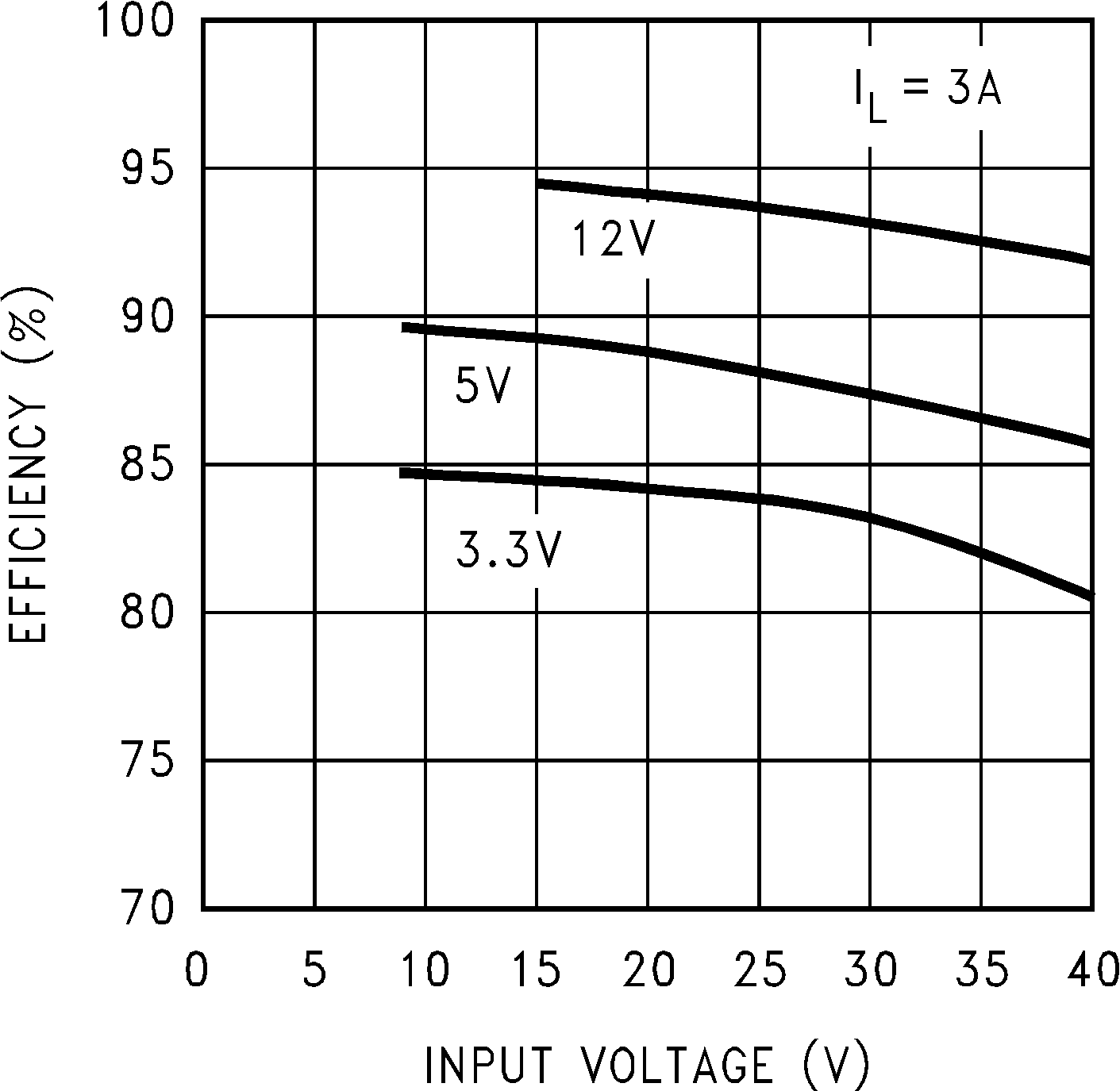 Figure 3. Efficiency vs Input Voltage
 Figure 5. Switch Current Limit
 Figure 7. Switching Frequency

| Continuous Mode Switching Waveforms VIN = 20 V, VOUT = 5 V, ILOAD = 3 A L = 33 µH, COUT = 200 µF, COUTESR = 26 mΩ |
||
| A: VSW Pin Voltage, 10 V/div | ||
| B: Inductor Current, 1 A/div | ||
| C: Output Ripple Voltage, 20 mV/div AC-Coupled |
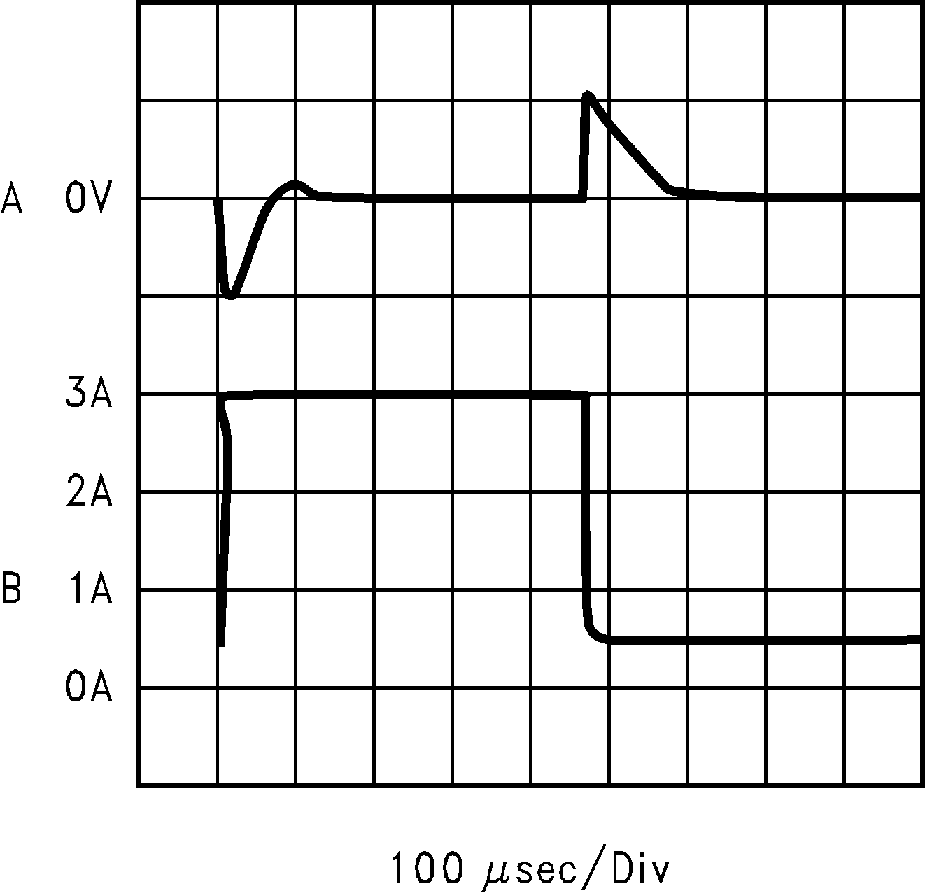
| Load Transient Response for Continuous Mode VIN = 20 V, VOUT = 5 V L = 33 µH, COUT = 200 µF, COUTESR = 26 mΩ |
||
| A: Output Voltage, 100 mV//div, AC-Coupled. | ||
| B: Load Current: 500-mA to 3-A Load Pulse |
 Figure 2. Line Regulation
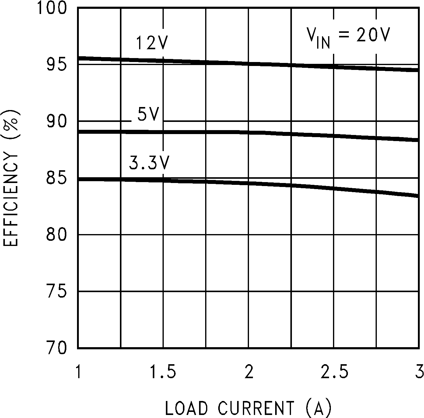 Figure 4. Efficiency vs ILOAD
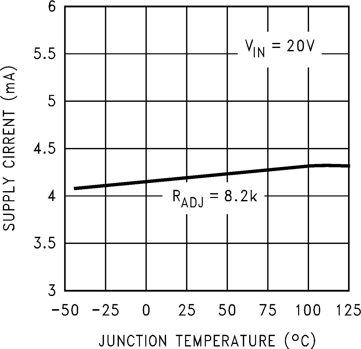 Figure 6. Operating Quiescent Current
 Figure 8. Feedback Pin Bias Current

| Discontinuous Mode Switching Waveforms VIN = 20 V, VOUT = 5 V, ILOAD = 500 mA L = 10 µH, COUT = 400 µF, COUTESR = 13 mΩ |
||
| A: VSW Pin Voltage, 10 V/div | ||
| B: Inductor Current, 1 A/div | ||
| C: Output Ripple Voltage, 20 mV/div AC-Coupled |

| Load Transient Response for Discontinuous Mode VIN = 20 V, VOUT = 5 V, L = 10 µH, COUT = 400 µF, COUTESR = 13 mΩ | ||
| A: Output Voltage, 100 mV/div, AC-Coupled. | ||
| B: Load Current: 200-mA to 3-A Load Pulse |
7 Detailed Description
7.1 Overview
The LM2673 provides all of the active functions required for a step-down (buck) switching regulator. The internal power switch is a DMOS power MOSFET to provide power supply designs with high current capability, up to 3 A, and highly efficient operation.
The design support WEBENCH, can also be used to provide instant component selection, circuit performance calculations for evaluation, a bill of materials component list and a circuit schematic for LM2673.
7.2 Functional Block Diagram
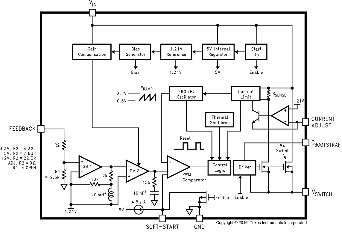
† Active Capacitor Patent Number 5,382,918
7.3 Feature Description
7.3.1 Switch Output
This is the output of a power MOSFET switch connected directly to the input voltage. The switch provides energy to an inductor, an output capacitor and the load circuitry under control of an internal pulse-width-modulator (PWM). The PWM controller is internally clocked by a fixed 260-kHz oscillator. In a standard step-down application the duty cycle (Time ON/Time OFF) of the power switch is proportional to the ratio of the power supply output voltage to the input voltage. The voltage on pin 1 switches between VIN (switch ON) and below ground by the voltage drop of the external Schottky diode (switch OFF).
7.3.2 Input
The input voltage for the power supply is connected to pin 2. In addition to providing energy to the load the input voltage also provides bias for the internal circuitry of the LM2673. For ensured performance the input voltage must be in the range of 8 V to 40 V. For best performance of the power supply the input pin must always be bypassed with an input capacitor located close to pin 2.
7.3.3 C Boost
A capacitor must be connected from pin 3 to the switch output, pin 1. This capacitor boosts the gate drive to the internal MOSFET above VIN to fully turn it ON. This minimizes conduction losses in the power switch to maintain high efficiency. The recommended value for C Boost is 0.01 µF.
7.3.4 Ground
This is the ground reference connection for all components in the power supply. In fast-switching, high-current applications such as those implemented with the LM2673, TI recommends that a broad ground plane be used to minimize signal coupling throughout the circuit.
7.3.5 Current Adjust
A key feature of the LM2673 is the ability to tailor the peak switch current limit to a level required by a particular application. This alleviates the need to use external components that must be physically sized to accommodate current levels (under shorted output conditions for example) that may be much higher than the normal circuit operating current requirements.
A resistor connected from pin 5 to ground establishes a current (I(pin 5) = 1.2 V / RADJ) that sets the peak current through the power switch. The maximum switch current is fixed at a level of 37,125 / RADJ.
7.3.6 Feedback
This is the input to a two-stage high gain amplifier, which drives the PWM controller. It is necessary to connect pin 6 to the actual output of the power supply to set the DC output voltage. For the fixed output devices (3.3-V, 5-V, and 12-V outputs), a direct wire connection to the output is all that is required as internal gain setting resistors are provided inside the LM2673. For the adjustable output version two external resistors are required to set the dc output voltage. For stable operation of the power supply it is important to prevent coupling of any inductor flux to the feedback input.
7.4 Device Functional Modes
7.4.1 Soft-Start
A capacitor connected from pin 7 to ground allows for a slow turnon of the switching regulator. The capacitor sets a time delay to gradually increase the duty cycle of the internal power switch. This can significantly reduce the amount of surge current required from the input supply during an abrupt application of the input voltage. If soft start is not required this pin must be left open circuited. See CSS Soft-Start Capacitor for further information regarding soft-start capacitor values.
8 Application and Implementation
NOTE
Information in the following applications sections is not part of the TI component specification, and TI does not warrant its accuracy or completeness. TI’s customers are responsible for determining suitability of components for their purposes. Customers should validate and test their design implementation to confirm system functionality.
8.1 Application Information
8.1.1 Design Considerations
Power supply design using the LM2673 is greatly simplified by using recommended external components. A wide range of inductors, capacitors and Schottky diodes from several manufacturers have been evaluated for use in designs that cover the full range of capabilities (input voltage, output voltage, and load current) of the LM2673. A simple design procedure using nomographs and component tables provided in this data sheet leads to a working design with very little effort.
The individual components from the various manufacturers called out for use are still just a small sample of the vast array of components available in the industry. While these components are recommended, they are not exclusively the only components for use in a design. After a close comparison of component specifications, equivalent devices from other manufacturers could be substituted for use in an application.
Important considerations for each external component and an explanation of how the nomographs and selection tables were developed follows.
8.1.2 Inductor
The inductor is the key component in a switching regulator. For efficiency the inductor stores energy during the switch ON time and then transfers energy to the load while the switch is OFF.
Nomographs are used to select the inductance value required for a given set of operating conditions. The nomographs assume that the circuit is operating in continuous mode (the current flowing through the inductor never falls to zero). The magnitude of inductance is selected to maintain a maximum ripple current of 30% of the maximum load current. If the ripple current exceeds this 30% limit the next larger value is selected.
The inductors offered have been specifically manufactured to provide proper operation under all operating conditions of input and output voltage and load current. Several part types are offered for a given amount of inductance. Both surface mount and through-hole devices are available. The inductors from each of the three manufacturers have unique characteristics.
- Renco: ferrite stick core inductors; benefits are typically lowest cost and can withstand ripple and transient peak currents above the rated value. These inductors have an external magnetic field, which may generate EMI.
- Pulse Engineering: powdered iron toroid core inductors; these also can withstand higher than rated currents and, being toroid inductors, has low EMI.
- Coilcraft: ferrite drum core inductors; these are the smallest physical size inductors and are available only as surface mount components. These inductors also generate EMI but less than stick inductors.
8.1.3 Output Capacitor
The output capacitor acts to smooth the dc output voltage and also provides energy storage. Selection of an output capacitor, with an associated equivalent series resistance (ESR), impacts both the amount of output ripple voltage and stability of the control loop.
The output ripple voltage of the power supply is the product of the capacitor ESR and the inductor ripple current. The capacitor types recommended in the tables were selected for having low ESR ratings.
In addition, both surface mount tantalum capacitors and through-hole aluminum electrolytic capacitors are offered as solutions.
Impacting frequency stability of the overall control loop, the output capacitance, in conjunction with the inductor, creates a double pole inside the feedback loop. In addition the capacitance and the ESR value create a zero. These frequency response effects together with the internal frequency compensation circuitry of the LM2673 modify the gain and phase shift of the closed loop system.
As a general rule for stable switching regulator circuits it is desired to have the unity gain bandwidth of the circuit to be limited to no more than one-sixth of the controller switching frequency. With the fixed 260-kHz switching frequency of the LM2673, the output capacitor is selected to provide a unity gain bandwidth of 40 kHz (maximum). Each recommended capacitor value has been chosen to achieve this result.
In some cases multiple capacitors are required either to reduce the ESR of the output capacitor, to minimize output ripple (a ripple voltage of 1% of VOUT or less is the assumed performance condition), or to increase the output capacitance to reduce the closed-loop unity gain bandwidth, to less than 40 kHz. When parallel combinations of capacitors are required it has been assumed that each capacitor is the exact same part type.
The RMS current and working voltage (WV) ratings of the output capacitor are also important considerations. In a typical step-down switching regulator, the inductor ripple current (set to be no more than 30% of the maximum load current by the inductor selection) is the current that flows through the output capacitor. The capacitor RMS current rating must be greater than this ripple current. The voltage rating of the output capacitor must be greater than 1.3 times the maximum output voltage of the power supply. If operation of the system at elevated temperatures is required, the capacitor voltage rating may be de-rated to less than the nominal room temperature rating. Careful inspection of the manufacturer's specification for de-rating of working voltage with temperature is important.
8.1.4 Input Capacitor
Fast changing currents in high current switching regulators place a significant dynamic load on the unregulated power source. An input capacitor helps to provide additional current to the power supply as well as smooth out input voltage variations.
Like the output capacitor, the key specifications for the input capacitor are RMS current rating and working voltage. The RMS current flowing through the input capacitor is equal to one-half of the maximum DC load current so the capacitor should be rated to handle this. Paralleling multiple capacitors proportionally increases the current rating of the total capacitance. The voltage rating must also be selected to be 1.3 times the maximum input voltage. Depending on the unregulated input power source, under light load conditions the maximum input voltage could be significantly higher than normal operation. Consider this when selecting an input capacitor.
The input capacitor must be placed very close to the input pin of the LM2673. Due to relative high current operation with fast transient changes, the series inductance of input connecting wires or PCB traces can create ringing signals at the input terminal which could possibly propagate to the output or other parts of the circuitry. It may be necessary in some designs to add a small valued (0.1 µF to 0.47 µF) ceramic type capacitor in parallel with the input capacitor to prevent or minimize any ringing.
8.1.5 Catch Diode
When the power switch in the LM2673 turns OFF, the current through the inductor continues to flow. The path for this current is through the diode connected between the switch output and ground. This forward biased diode clamps the switch output to a voltage less than ground. This negative voltage must be greater than –1 V so a low voltage drop (particularly at high current levels) Schottky diode is recommended. Total efficiency of the entire power supply is significantly impacted by the power lost in the output catch diode. The average current through the catch diode is dependent on the switch duty cycle (D) and is equal to the load current times (1-D). Use of a diode rated for much higher current than is required by the actual application helps to minimize the voltage drop and power loss in the diode.
During the switch ON time the diode will be reversed biased by the input voltage. The reverse voltage rating of the diode should be at least 1.3 times greater than the maximum input voltage.
8.1.6 Boost Capacitor
The boost capacitor creates a voltage used to overdrive the gate of the internal power MOSFET. This improves efficiency by minimizing the on resistance of the switch and associated power loss. For all applications it is recommended to use a 0.01-µF, 50-V ceramic capacitor.
8.1.7 RADJ, Adjustable Current Limit
A key feature of the LM2673 is the ability to control the peak switch current. Without this feature the peak switch current would be internally set to 5 A or higher to accommodate 3-A load current designs. This requires that both the inductor (which could saturate with excessively high currents) and the catch diode be able to safely handle up to 5 A which would be conducted under load fault conditions.
If an application only requires a load current of 2 A or so the peak switch current can be set to a limit just over the maximum load current with the addition of a single programming resistor. This allows the use of less powerful and more cost-effective inductors and diodes.
The peak switch current is equal to a factor of 37,125 divided by RADJ. A resistance of 8.2 kΩ sets the current limit to typically 4.5 A. For predictable control of the current limit, TI recommends keeping the peak switch current greater than 1 A. For lower current applications 500-mA and 1-A switching regulators, the LM2674 and LM2672, are available.
When the power switch reaches the current limit threshold it is immediately turned OFF and the internal switching frequency is reduced. This extends the OFF time of the switch to prevent a steady-state, high-current condition. As the switch current falls below the current limit threshold, the switch turns back ON. If a load fault continues, the switch again exceeds the threshold and switch back OFF. This results in a low duty cycle pulsing of the power switch to minimize the overall fault condition power dissipation.
8.1.8 CSS Soft-Start Capacitor
This optional capacitor controls the rate at which the LM2673 starts up at power on. The capacitor is charged linearly by an internal current source. This voltage ramp gradually increases the duty cycle of the power switch until it reaches the normal operating duty cycle defined primarily by the ratio of the output voltage to the input voltage. The soft-start turnon time is programmable by the selection of CSS.
The formula for selecting a soft-start capacitor is:

where
- ISST = Soft-start current, 3.7 µA typical
- tSS = Soft-start time, from design requirements
- VSST = Soft-start threshold voltage, 0.63 V typical
- VOUT = Output voltage, from design requirements
- VSCHOTTKY = Schottky diode voltage drop, typically 0.5 V
- VIN = Maximum input voltage, from design requirements
If this feature is not desired, leave the soft-start pin (pin 7) open circuited.
With certain soft-start capacitor values and operating conditions, the LM2673 can exhibit an overshoot on the output voltage during turnon. Especially when starting up into no load or low load, the soft-start function may not be effective in preventing a larger voltage overshoot on the output. With larger loads or lower input voltages during start-up this effect is minimized. In particular, avoid using soft-start capacitors between 0.033 µF and 1 µF.
8.1.9 Additional Application Information
When the output voltage is greater than approximately 6 V, and the duty cycle at minimum input voltage is greater than approximately 50%, the designer should exercise caution in selection of the output filter components. When an application designed to these specific operating conditions is subjected to a current limit fault condition, it may be possible to observe a large hysteresis in the current limit. This can affect the output voltage of the device until the load current is reduced sufficiently to allow the current limit protection circuit to reset itself.
Under current limiting conditions, the LM267x is designed to respond in the following manner:
- At the moment when the inductor current reaches the current limit threshold, the ON-pulse is immediately terminated. This happens for any application condition.
- However, the current limit block is also designed to momentarily reduce the duty cycle to below 50% to avoid subharmonic oscillations, which could cause the inductor to saturate.
- Thereafter, once the inductor current falls below the current limit threshold, there is a small relaxation time during which the duty cycle progressively rises back above 50% to the value required to achieve regulation.
If the output capacitance is sufficiently large, it may be possible that as the output tries to recover, the output capacitor charging current is large enough to repeatedly re-trigger the current-limit circuit before the output has fully settled. This condition is exacerbated with higher output voltage settings because the energy requirement of the output capacitor varies as the square of the output voltage (½ CV2), thus requiring an increased charging current.
A simple test to determine if this condition might exist for a suspect application is to apply a short circuit across the output of the converter, and then remove the shorted output condition. In an application with properly selected external components, the output recovers smoothly.
Practical values of external components that have been experimentally found to work well under these specific operating conditions are COUT = 47 µF, L = 22 µH. It should be noted that even with these components, for a device’s current limit of ICLIM, the maximum load current under which the possibility of the large current limit hysteresis can be minimized is ICLIM / 2. For example, if the input is 24 V and the set output voltage is 18 V, then for a desired maximum current of 1.5 A, the current limit of the chosen switcher must be confirmed to be at least 3 A.
Under extreme overcurrent or short-circuit conditions, the LM267X employs frequency foldback in addition to the current limit. If the cycle-by-cycle inductor current increases above the current limit threshold (due to short circuit or inductor saturation for example) the switching frequency is automatically reduced to protect the IC. Frequency below 100 kHz is typical for an extreme short-circuit condition.
8.2 Typical Applications
8.2.1 Typical Application for All Output Voltage Versions
 Figure 13. Basic Circuit for All Output Voltage Versions
8.2.1.1 Design Requirements
Select the power supply operating conditions and the maximum output current and follow below procedures to find the external components for LM2673.
8.2.1.2 Detailed Design Procedure
Using the nomographs and tables in this data sheet (or use the available design software at www.ti.com) a complete step-down regulator can be designed in a few simple steps.
Step 1: Define the power supply operating conditions:
- Required output voltage
- Maximum DC input voltage
- Maximum output load current
Step 2: Set the output voltage by selecting a fixed output LM2673 (3.3-V, 5-V, or 12-V applications) or determine the required feedback resistors for use with the adjustable LM2673-ADJ
Step 3: Determine the inductor required by using one of the four nomographs, Figure 14 through Figure 17. Table 3 provides a specific manufacturer and part number for the inductor.
Step 4: Using Table 5 and Table 6 (fixed output voltage) or Table 9 and Table 10 (adjustable output voltage), determine the output capacitance required for stable operation. Table 1 and Table 10 provide the specific capacitor type from the manufacturer of choice.
Step 5: Determine an input capacitor from Table 5 and Table 8 for fixed output voltage applications. Use Table 1 or Table 2 to find the specific capacitor type. For adjustable output circuits select a capacitor from Table 1 or Table 2 with a sufficient working voltage (WV) rating greater than VIN maximum, and an RMS current rating greater than one-half the maximum load current (2 or more capacitors in parallel may be required).
Step 6:Select an appropriate diode from Table 4. The current rating of the diode must be greater than ILOAD maximum and the reverse voltage rating must be greater than VIN maximum.
Step 7: Include a 0.01-µF, 50-V capacitor for CBOOSTin the design and then determine the value of a soft-start capacitor if desired.
Step 8: Define a value for RADJ to set the peak switch current limit to be at least 20% greater than IOUT maximum to allow for at least 30% inductor ripple current (±15% of IOUT). For designs that must operate over the full temperature range the switch current limit should be set to at least 50% greater than IOUT maximum (1.5 × IOUT maximum).
8.2.1.2.1 Capacitor Selection Guides
Table 1. Input and Output Capacitor Codes—Surface Mount
| CAPACITOR REFERENCE CODE | SURFACE MOUNT | ||||||||
|---|---|---|---|---|---|---|---|---|---|
| AVX TPS SERIES | SPRAGUE 594D SERIES | KEMET T495 SERIES | |||||||
| C (µF) | WV (V) | Irms (A) | C (µF) | WV (V) | Irms (A) | C (µF) | WV (V) | Irms (A) | |
| C1 | 330 | 6.3 | 1.15 | 120 | 6.3 | 1.1 | 100 | 6.3 | 0.82 |
| C2 | 100 | 10 | 1.1 | 220 | 6.3 | 1.4 | 220 | 6.3 | 1.1 |
| C3 | 220 | 10 | 1.15 | 68 | 10 | 1.05 | 330 | 6.3 | 1.1 |
| C4 | 47 | 16 | 0.89 | 150 | 10 | 1.35 | 100 | 10 | 1.1 |
| C5 | 100 | 16 | 1.15 | 47 | 16 | 1 | 150 | 10 | 1.1 |
| C6 | 33 | 20 | 0.77 | 100 | 16 | 1.3 | 220 | 10 | 1.1 |
| C7 | 68 | 20 | 0.94 | 180 | 16 | 1.95 | 33 | 20 | 0.78 |
| C8 | 22 | 25 | 0.77 | 47 | 20 | 1.15 | 47 | 20 | 0.94 |
| C9 | 10 | 35 | 0.63 | 33 | 25 | 1.05 | 68 | 20 | 0.94 |
| C10 | 22 | 35 | 0.66 | 68 | 25 | 1.6 | 10 | 35 | 0.63 |
| C11 | — | — | — | 15 | 35 | 0.75 | 22 | 35 | 0.63 |
| C12 | — | — | — | 33 | 35 | 1 | 4.7 | 50 | 0.66 |
| C13 | — | — | — | 15 | 50 | 0.9 | — | — | — |
Table 2. Input and Output Capacitor Codes—Through Hole
| CAPACITOR REFERENCE CODE | THROUGH HOLE | |||||||||||
|---|---|---|---|---|---|---|---|---|---|---|---|---|
| SANYO OS-CON SA SERIES | SANYO MV-GX SERIES | NICHICON PL SERIES | PANASONIC HFQ SERIES | |||||||||
| C (µF) | WV (V) | Irms (A) | C (µF) | WV (V) | Irms (A) | C (µF) | WV (V) | Irms (A) | C (µF) | WV (V) | Irms (A) | |
| C1 | 47 | 6.3 | 1 | 1000 | 6.3 | 0.8 | 680 | 10 | 0.8 | 82 | 35 | 0.4 |
| C2 | 150 | 6.3 | 1.95 | 270 | 16 | 0.6 | 820 | 10 | 0.98 | 120 | 35 | 0.44 |
| C3 | 330 | 6.3 | 2.45 | 470 | 16 | 0.75 | 1000 | 10 | 1.06 | 220 | 35 | 0.76 |
| C4 | 100 | 10 | 1.87 | 560 | 16 | 0.95 | 1200 | 10 | 1.28 | 330 | 35 | 1.01 |
| C5 | 220 | 10 | 2.36 | 820 | 16 | 1.25 | 2200 | 10 | 1.71 | 560 | 35 | 1.4 |
| C6 | 33 | 16 | 0.96 | 1000 | 16 | 1.3 | 3300 | 10 | 2.18 | 820 | 35 | 1.62 |
| C7 | 100 | 16 | 1.92 | 150 | 35 | 0.65 | 3900 | 10 | 2.36 | 1000 | 35 | 1.73 |
| C8 | 150 | 16 | 2.28 | 470 | 35 | 1.3 | 6800 | 10 | 2.68 | 2200 | 35 | 2.8 |
| C9 | 100 | 20 | 2.25 | 680 | 35 | 1.4 | 180 | 16 | 0.41 | 56 | 50 | 0.36 |
| C10 | 47 | 25 | 2.09 | 1000 | 35 | 1.7 | 270 | 16 | 0.55 | 100 | 50 | 0.5 |
| C11 | — | — | — | 220 | 63 | 0.76 | 470 | 16 | 0.77 | 220 | 50 | 0.92 |
| C12 | — | — | — | 470 | 63 | 1.2 | 680 | 16 | 1.02 | 470 | 50 | 1.44 |
| C13 | — | — | — | 680 | 63 | 1.5 | 820 | 16 | 1.22 | 560 | 50 | 1.68 |
| C14 | — | — | — | 1000 | 63 | 1.75 | 1800 | 16 | 1.88 | 1200 | 50 | 2.22 |
| C15 | — | — | — | — | — | — | 220 | 25 | 0.63 | 330 | 63 | 1.42 |
| C16 | — | — | — | — | — | — | 220 | 35 | 0.79 | 1500 | 63 | 2.51 |
| C17 | — | — | — | — | — | — | 560 | 35 | 1.43 | — | — | — |
| C18 | — | — | — | — | — | — | 2200 | 35 | 2.68 | — | — | — |
| C19 | — | — | — | — | — | — | 150 | 50 | 0.82 | — | — | — |
| C20 | — | — | — | — | — | — | 220 | 50 | 1.04 | — | — | — |
| C21 | — | — | — | — | — | — | 330 | 50 | 1.3 | — | — | — |
| C22 | — | — | — | — | — | — | 100 | 63 | 0.75 | — | — | — |
| C23 | — | — | — | — | — | — | 390 | 63 | 1.62 | — | — | — |
| C24 | — | — | — | — | — | — | 820 | 63 | 2.22 | — | — | — |
| C25 | — | — | — | — | — | — | 1200 | 63 | 2.51 | — | — | — |
8.2.1.2.2 Inductor Selection Guide
Table 3. Inductor Manufacturer Part Numbers
| INDUCTOR REFERENCE NUMBER | INDUCTANCE (µH) | CURRENT (A) | RENCO | PULSE ENGINEERING | COILCRAFT | ||
|---|---|---|---|---|---|---|---|
| THROUGH HOLE | SURFACE MOUNT | THROUGH HOLE | SURFACE MOUNT | SURFACE MOUNT | |||
| L23 | 33 | 1.35 | RL-5471-7 | RL1500-33 | PE-53823 | PE-53823S | DO3316-333 |
| L24 | 22 | 1.65 | RL-1283-22-43 | RL1500-22 | PE-53824 | PE-53824S | DO3316-223 |
| L25 | 15 | 2 | RL-1283-15-43 | RL1500-15 | PE-53825 | PE-53825S | DO3316-153 |
| L29 | 100 | 1.41 | RL-5471-4 | RL-6050-100 | PE-53829 | PE-53829S | DO5022P-104 |
| L30 | 68 | 1.71 | RL-5471-5 | RL6050-68 | PE-53830 | PE-53830S | DO5022P-683 |
| L31 | 47 | 2.06 | RL-5471-6 | RL6050-47 | PE-53831 | PE-53831S | DO5022P-473 |
| L32 | 33 | 2.46 | RL-5471-7 | RL6050-33 | PE-53932 | PE-53932S | DO5022P-333 |
| L33 | 22 | 3.02 | RL-1283-22-43 | RL6050-22 | PE-53933 | PE-53933S | DO5022P-223 |
| L34 | 15 | 3.65 | RL-1283-15-43 | — | PE-53934 | PE-53934S | DO5022P-153 |
| L38 | 68 | 2.97 | RL-5472-2 | — | PE-54038 | PE-54038S | — |
| L39 | 47 | 3.57 | RL-5472-3 | — | PE-54039 | PE-54039S | — |
| L40 | 33 | 4.26 | RL-1283-33-43 | — | PE-54040 | PE-54040S | — |
| L41 | 22 | 5.22 | RL-1283-22-43 | — | PE-54041 | P0841 | — |
| L44 | 68 | 3.45 | RL-5473-3 | — | PE-54044 | — | — |
| L45 | 10 | 4.47 | RL-1283-10-43 | — | — | P0845 | DO5022P-103HC |
Table 4. Schottky Diode Selection Table
| REVERSE VOLTAGE (V) | SURFACE MOUNT | THROUGH HOLE | ||
|---|---|---|---|---|
| 3 A | 5 A OR MORE | 3 A | 5 A OR MORE | |
| 20 | SK32 | — | 1N5820 | — |
| SR302 | ||||
| 30 | SK33 | MBRD835L | 1N5821 | — |
| 30WQ03F | 31DQ03 | |||
| 40 | SK34 | MBRB1545CT | 1N5822 | — |
| 30BQ040 | 6TQ045S | MBR340 | MBR745 | |
| 30WQ04F | 31DQ04 | 80SQ045 | ||
| MBRS340 | SR403 | 6TQ045 | ||
| MBRD340 | ||||
| 50 or more | SK35 | — | MBR350 | — |
| 30WQ05F | 31DQ05 | |||
| SR305 | ||||
8.2.1.3 Application Curves
For Continuous Mode Operation
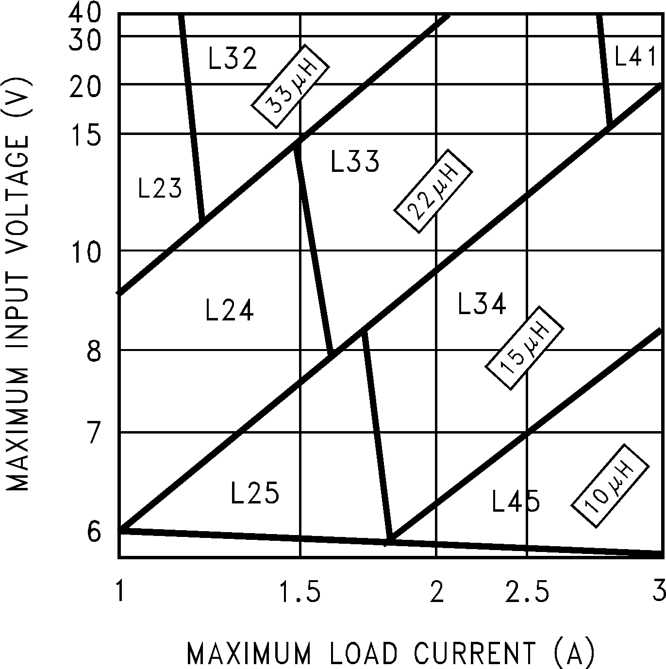 Figure 14. LM2673-3.3
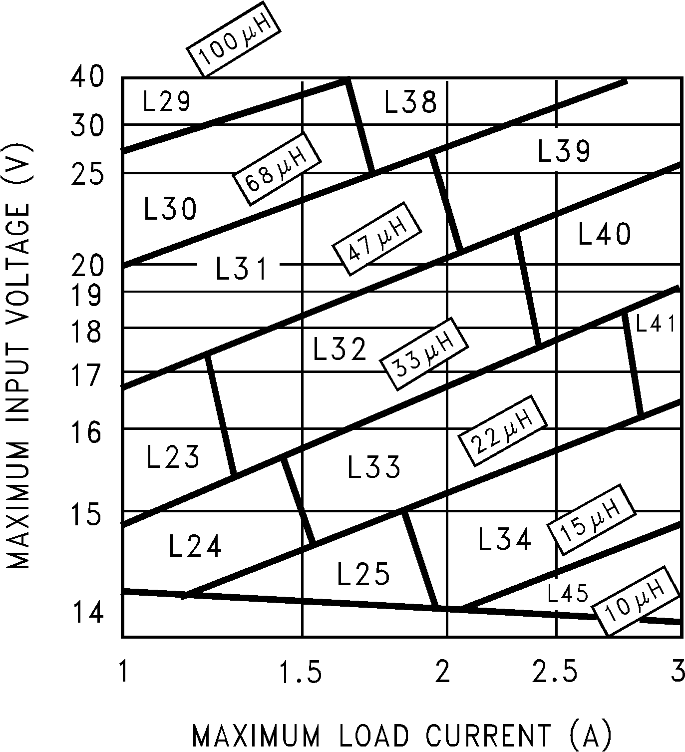 Figure 16. LM2673-12
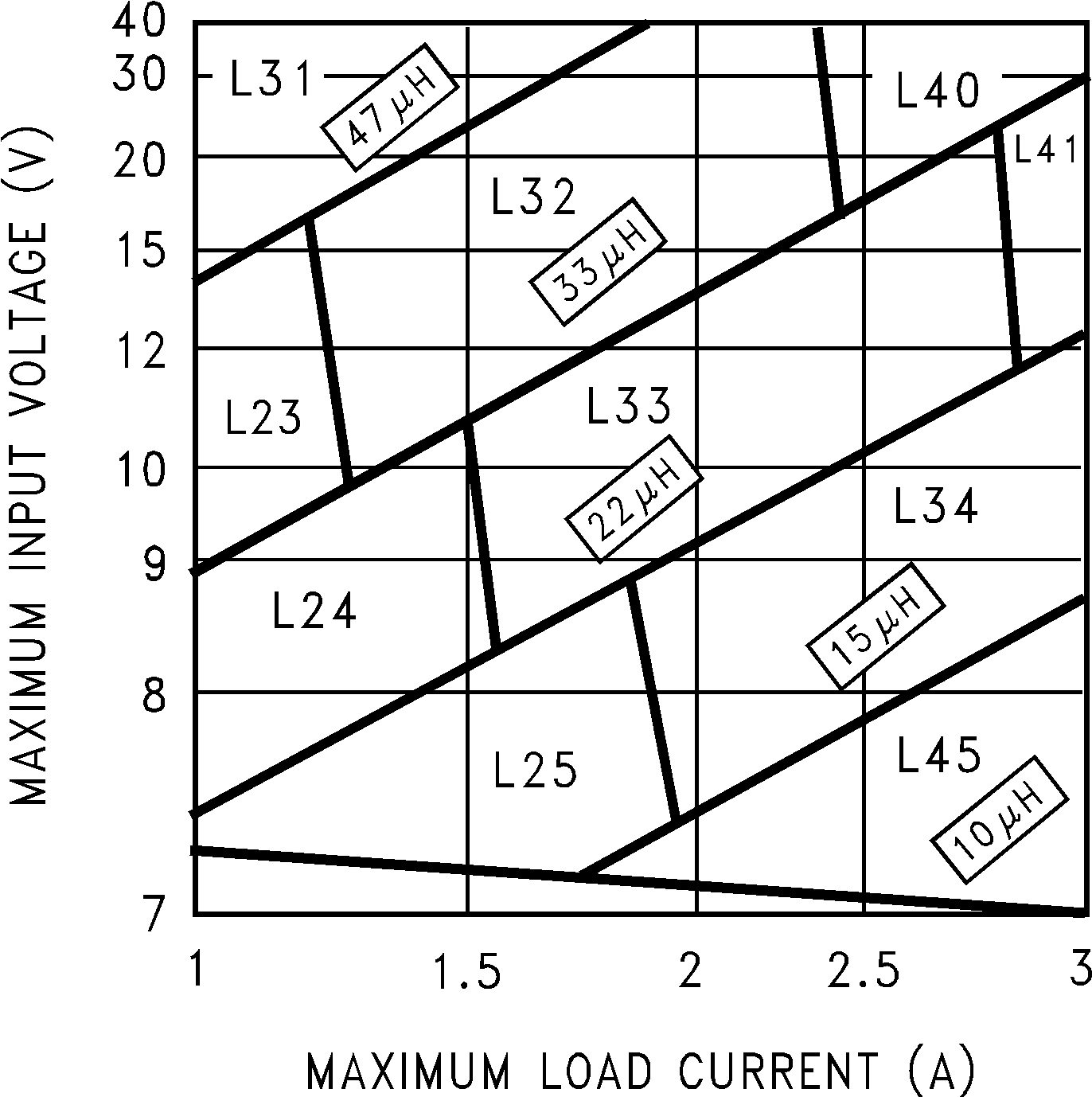 Figure 15. LM2673-5
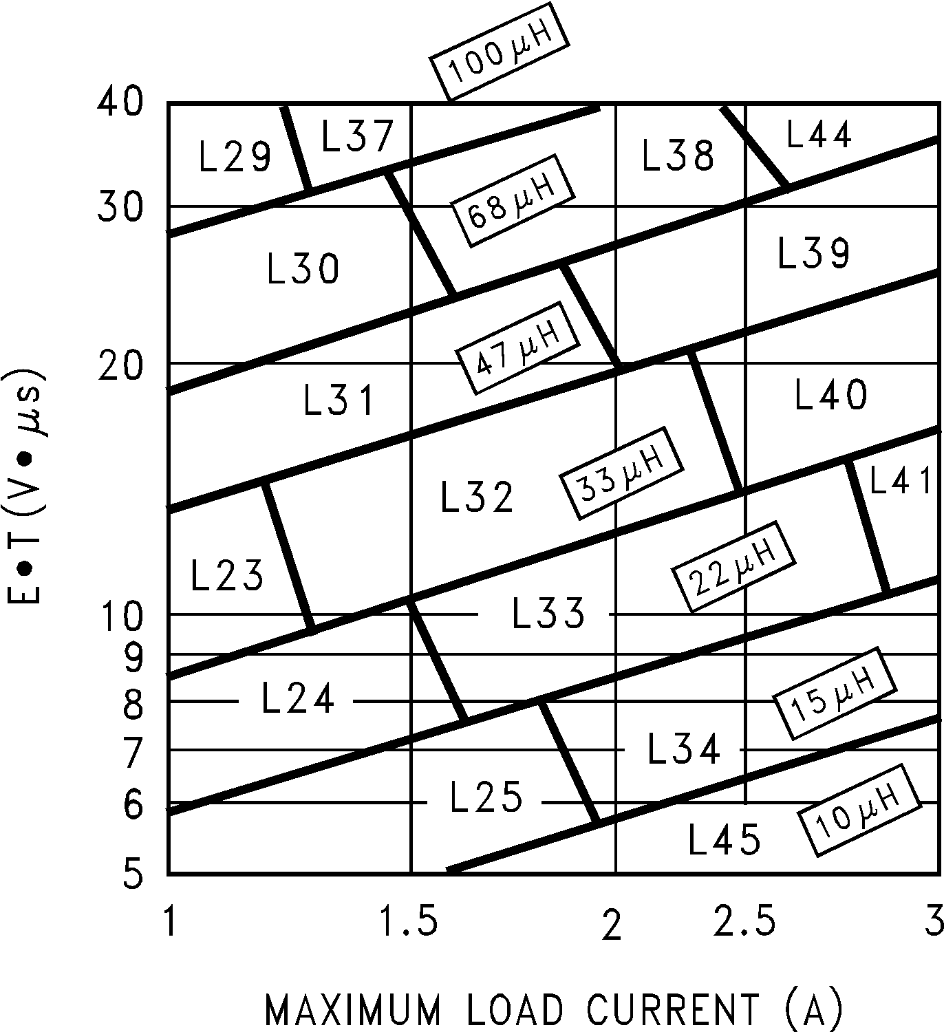 Figure 17. LM2673-ADJ
8.2.2 Fixed Output Voltage Application
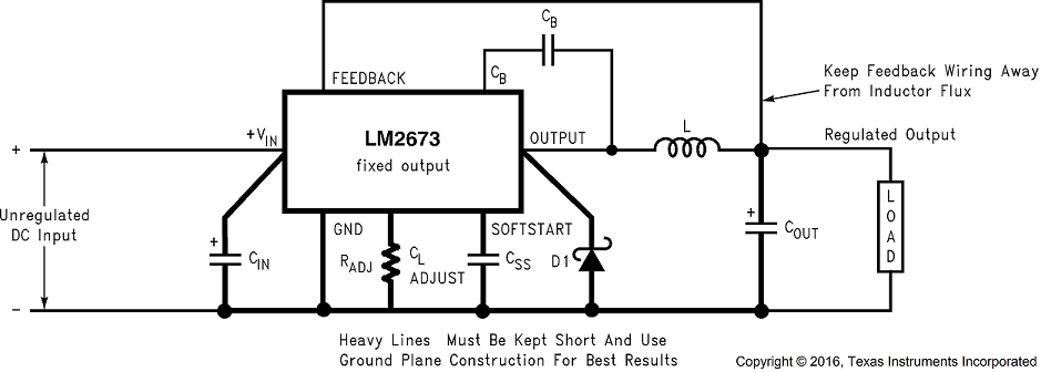 Figure 18. Basic Circuit for Fixed Output Voltage Applications
8.2.2.1 Design Requirements
Select the power supply operating conditions and the maximum output current and follow below procedures to find the external components for LM2673.
8.2.2.2 Detailed Design Procedure
A system logic power supply bus of 3.3 V is to be generated from a wall adapter which provides an unregulated DC voltage of 13 V to 16 V. The maximum load current is 2.5 A. A soft-start delay time of 50 ms is desired. Through-hole components are preferred.
Step 1: Operating conditions are:
- VOUT = 3.3 V
- VIN maximum = 16 V
- ILOAD maximum = 2.5 A
Step 2: Select an LM2673T-3.3. The output voltage has a tolerance of ±2% at room temperature and ±3% over the full operating temperature range.
Step 3: Use the nomograph for the 3.3-V device, Figure 14. The intersection of the 16-V horizontal line (VIN max) and the 2.5-A vertical line (ILOAD max) indicates that L33, a 22-µH inductor, is required.
From Table 3, L33 in a through-hole component is available from Renco with part number RL-1283-22-43 or part number PE-53933 from Pulse Engineering.
Step 4: Use Table 5 or Table 6 to determine an output capacitor. With a 3.3-V output and a 33-µH inductor there are four through-hole output capacitor solutions with the number of same type capacitors to be paralleled and an identifying capacitor code given. Table 1 or Table 2 provide the actual capacitor characteristics. Any of the following choices will work in the circuit:
- 1 × 220-µF, 10-V Sanyo OS-CON (code C5)
- 1 × 1000-µF, 35-V Sanyo MV-GX (code C10)
- 1 × 2200-µF, 10-V Nichicon PL (code C5)
- 1 × 1000-µF, 35-V Panasonic HFQ (code C7)
Step 5:Use Table 5 or Table 8 to select an input capacitor. With 3.3-V output and 22 µH there are three through-hole solutions. These capacitors provide a sufficient voltage rating and an RMS current rating greater than 1.25 A (1/2 ILOAD max). Again using Table 1 or Table 2 for specific component characteristics the following choices are suitable:
- 1 × 1000-µF, 63-V Sanyo MV-GX (code C14)
- 1 × 820-µF, 63-V Nichicon PL (code C24)
- 1 × 560-µF, 50-V Panasonic HFQ (code C13)
Step 6: From Table 4 a 3-A or more Schottky diode must be selected. The 20-V rated diodes are sufficient for the application and for through-hole components two part types are suitable:
- 1N5820
- SR302
Step 7: A 0.01-µF capacitor will be used for CBOOST. For the 50-ms soft-start delay the following parameters are to be used:
- ISST: 3.7 µA
- tSS: 50 mS
- VSST: 0.63 V
- VOUT: 3.3 V
- VSCHOTTKY: 0.5 V
- VIN: 16 V
Using VIN max ensures that the soft-start delay time will be at least the desired 50 ms.
Using the formula for CSS a value of 0.148 µF is determined to be required. Use of a standard value 0.22-µF capacitor will produce more than sufficient soft-start delay.
Step 8: Determine a value for RADJ to provide a peak switch current limit of at least 2.5 A plus 50% or 3.75 A.

Use a value of 10 kΩ.
8.2.2.2.1 Capacitor Selection
Table 5. Output Capacitors for Fixed Output Voltage Application—Surface Mount(1)(2)
| OUTPUT VOLTAGE (V) | INDUCTANCE (µH) | SURFACE MOUNT | |||||
|---|---|---|---|---|---|---|---|
| AVX TPS SERIES | SPRAGUE 594D SERIES | KEMET T495 SERIES | |||||
| NO. | C CODE | NO. | C CODE | NO. | C CODE | ||
| 3.3 | 10 | 4 | C2 | 3 | C1 | 4 | C4 |
| 15 | 4 | C2 | 3 | C1 | 4 | C4 | |
| 22 | 3 | C2 | 2 | C7 | 3 | C4 | |
| 33 | 2 | C2 | 2 | C6 | 2 | C4 | |
| 5 | 10 | 4 | C2 | 4 | C6 | 4 | C4 |
| 15 | 3 | C2 | 2 | C7 | 3 | C4 | |
| 22 | 3 | C2 | 2 | C7 | 3 | C4 | |
| 33 | 2 | C2 | 2 | C3 | 2 | C4 | |
| 47 | 2 | C2 | 1 | C7 | 2 | C4 | |
| 12 | 10 | 4 | C5 | 3 | C6 | 5 | C9 |
| 15 | 3 | C5 | 2 | C7 | 4 | C8 | |
| 22 | 2 | C5 | 2 | C6 | 3 | C8 | |
| 33 | 2 | C5 | 1 | C7 | 2 | C8 | |
| 47 | 2 | C4 | 1 | C6 | 2 | C8 | |
| 68 | 1 | C5 | 1 | C5 | 2 | C7 | |
| 100 | 1 | C4 | 1 | C5 | 1 | C8 | |
Table 6. Output Capacitors for Fixed Output Voltage Application—Through Hole(1)(2)
| OUTPUT VOLTAGE (V) | INDUCTANCE (µH) | THROUGH HOLE | |||||||
|---|---|---|---|---|---|---|---|---|---|
| SANYO OS-CON SA SERIES | SANYO MV-GX SERIES | NICHICON PL SERIES | PANASONIC HFQ SERIES | ||||||
| NO. | C CODE | NO. | C CODE | NO. | C CODE | NO. | C CODE | ||
| 3.3 | 10 | 1 | C3 | 1 | C10 | 1 | C6 | 2 | C6 |
| 15 | 1 | C3 | 1 | C10 | 1 | C6 | 2 | C5 | |
| 22 | 1 | C5 | 1 | C10 | 1 | C5 | 1 | C7 | |
| 33 | 1 | C2 | 1 | C10 | 1 | C13 | 1 | C5 | |
| 5 | 10 | 2 | C4 | 1 | C10 | 1 | C6 | 2 | C5 |
| 15 | 1 | C5 | 1 | C10 | 1 | C5 | 1 | C6 | |
| 22 | 1 | C5 | 1 | C5 | 1 | C5 | 1 | C5 | |
| 33 | 1 | C4 | 1 | C5 | 1 | C13 | 1 | C5 | |
| 47 | 1 | C4 | 1 | C4 | 1 | C13 | 2 | C3 | |
| 12 | 10 | 2 | C7 | 2 | C5 | 1 | C18 | 2 | C5 |
| 15 | 1 | C8 | 1 | C5 | 1 | C17 | 1 | C5 | |
| 22 | 1 | C7 | 1 | C5 | 1 | C13 | 1 | C5 | |
| 33 | 1 | C7 | 1 | C3 | 1 | C11 | 1 | C4 | |
| 47 | 1 | C7 | 1 | C3 | 1 | C10 | 1 | C3 | |
| 68 | 1 | C7 | 1 | C2 | 1 | C10 | 1 | C3 | |
| 100 | 1 | C7 | 1 | C2 | 1 | C9 | 1 | C1 | |
Table 7. Input Capacitors for Fixed Output Voltage Application—Surface Mount(1)(3)(4)
| OUTPUT VOLTAGE (V) | INDUCTANCE (µH) | SURFACE MOUNT | |||||
|---|---|---|---|---|---|---|---|
| AVX TPS SERIES | SPRAGUE 594D SERIES | KEMET T495 SERIES | |||||
| NO. | C CODE | NO. | C CODE | NO. | C CODE | ||
| 3.3 | 10 | 2 | C5 | 1 | C7 | 2 | C8 |
| 15 | 3 | C9 | 1 | C10 | 3 | C10 | |
| 22 | See(2) | See(2) | 2 | C13 | 3 | C12 | |
| 33 | See(2) | See(2) | 2 | C13 | 2 | C12 | |
| 5 | 10 | 2 | C5 | 1 | C7 | 2 | C8 |
| 15 | 2 | C5 | 1 | C7 | 2 | C8 | |
| 22 | 3 | C10 | 2 | C12 | 3 | C11 | |
| 33 | See(2) | See(2) | 2 | C13 | 3 | C12 | |
| 47 | See(2) | See(2) | 1 | C13 | 2 | C12 | |
| 12 | 10 | 2 | C7 | 2 | C10 | 2 | C7 |
| 15 | 2 | C7 | 2 | C10 | 2 | C7 | |
| 22 | 3 | C10 | 2 | C12 | 3 | C10 | |
| 33 | 3 | C10 | 2 | C12 | 3 | C10 | |
| 47 | See(2) | See(2) | 2 | C13 | 3 | C12 | |
| 68 | See(2) | See(2) | 2 | C13 | 2 | C12 | |
| 100 | See(2) | See(2) | 1 | C13 | 2 | C12 | |
Table 8. Input Capacitors for Fixed Output Voltage Application—Through Hole(1)(3)(4)
| OUTPUT VOLTAGE (V) | INDUCTANCE (µH) | THROUGH HOLE | |||||||
|---|---|---|---|---|---|---|---|---|---|
| SANYO OS-CON SA SERIES | SANYO MV-GX SERIES | NICHICON PL SERIES | PANASONIC HFQ SERIES | ||||||
| NO. | C CODE | NO. | C CODE | NO. | C CODE | NO. | C CODE | ||
| 3.3 | 10 | 1 | C7 | 2 | C4 | 1 | C5 | 1 | C6 |
| 15 | 1 | C10 | 1 | C10 | 1 | C18 | 1 | C6 | |
| 22 | See(2) | See(2) | 1 | C14 | 1 | C24 | 1 | C13 | |
| 33 | See(2) | See(2) | 1 | C12 | 1 | C20 | 1 | C12 | |
| 5 | 10 | 1 | C7 | 2 | C4 | 1 | C14 | 1 | C6 |
| 15 | 1 | C7 | 2 | C4 | 1 | C14 | 1 | C6 | |
| 22 | See(2) | See(2) | 1 | C10 | 1 | C18 | 1 | C13 | |
| 33 | See(2) | See(2) | 1 | C14 | 1 | C23 | 1 | C13 | |
| 47 | See(2) | See(2) | 1 | C12 | 1 | C20 | 1 | C12 | |
| 12 | 10 | 1 | C9 | 1 | C10 | 1 | C18 | 1 | C6 |
| 15 | 1 | C10 | 1 | C10 | 1 | C18 | 1 | C6 | |
| 22 | 1 | C10 | 1 | C10 | 1 | C18 | 1 | C6 | |
| 33 | See(2) | See(2) | 1 | C10 | 1 | C18 | 1 | C6 | |
| 47 | See(2) | See(2) | 1 | C13 | 1 | C23 | 1 | C13 | |
| 68 | See(2) | See(2) | 1 | C12 | 1 | C21 | 1 | C12 | |
| 100 | See(2) | See(2) | 1 | C11 | 1 | C22 | 1 | C11 | |
8.2.3 Adjustable Output Design Example
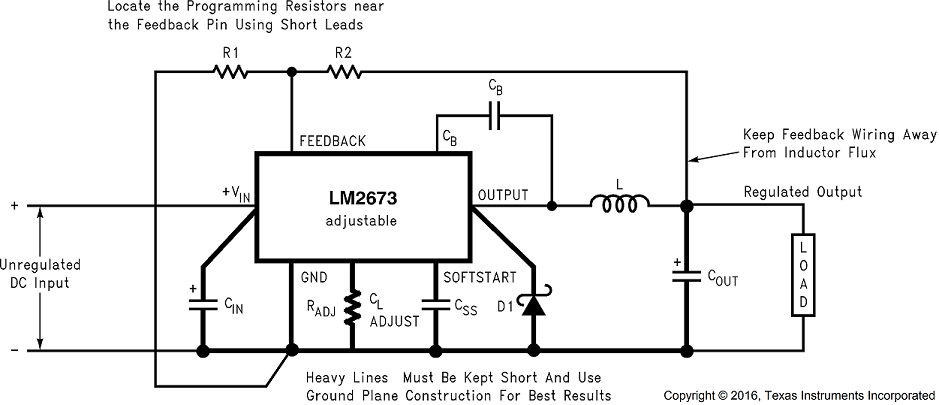 Figure 19. Basic Circuit for Adjustable Output Voltage Applications
8.2.3.1 Design Requirements
Select the power supply operating conditions and the maximum output current and follow below procedures to find the external components for LM2673.
8.2.3.2 Detailed Design Procedure
In this example, it is desired to convert the voltage from a two battery automotive power supply (voltage range of 20 V to 28 V, typical in large truck applications) to the 14.8-VDC alternator supply typically used to power electronic equipment from single battery 12-V vehicle systems. The load current required is 2 A (maximum). It is also desired to implement the power supply with all surface mount components. Soft start is not required.
Step 1: Operating conditions are:
- VOUT = 14.8 V
- VIN maximum = 28 V
- ILOAD maximum = 2 A
Step 2: Select an LM2673S-ADJ. To set the output voltage to 14.9 V, two resistors need to be chosen (R1 and R2 in Figure 19). For the adjustable device the output voltage is set by the following relationship:

where
- VFB is the feedback voltage of typically 1.21 V
A recommended value to use for R1 is 1kΩ. In this example then R2 is determined to be:

R2 = 11.23 kΩ
The closest standard 1% tolerance value to use is 11.3 kΩ
This sets the nominal output voltage to 14.88 V which is within 0.5% of the target value.
Step 3:To use the nomograph for the adjustable device, Figure 17, requires a calculation of the inductor Volt • microsecond constant (E • T expressed in V • µS) from the following formula:

where
- VSAT is the voltage drop across the internal power switch which is Rds(ON) times ILOAD
In this example this would be typically 0.15 Ω × 2 A or 0.3 V and VD is the voltage drop across the forward biased Schottky diode, typically 0.5 V. The switching frequency of 260 KHz is the nominal value to use to estimate the ON time of the switch during which energy is stored in the inductor.
For this example E • T is found to be:


Using Figure 17, the intersection of 27 V • µS horizontally and the 2-A vertical line (ILOAD max) indicates that L38, a 68-µH inductor, must be used.
From Table 3, L38 in a surface mount component is available from Pulse Engineering with part number PE-54038S.
Step 4: Use Table 9 or Table 10 to determine an output capacitor. With a 14.8-V output the 12.5-V to 15-V row is used and with a 68-µH inductor there are three surface mount output capacitor solutions. Table 1 or Table 2 provide the actual capacitor characteristics based on the C Code number. Any of the following choices can be used:
- 1 × 33-µF, 20-V AVX TPS (code C6)
- 1 × 47-µF, 20-V Sprague 594 (code C8)
- 1 × 47-µF, 20-V Kemet T495 (code C8)
NOTE
When using the adjustable device in low voltage applications (less than 3-V output), if the nomograph, Figure 17, selects an inductance of 22 µH or less, Table 9 and Table 10 do not provide an output capacitor solution. With these conditions the number of output capacitors required for stable operation becomes impractical. TI recommends either a 33-µH or 47-µH inductor and the output capacitors from Table 9 or Table 10.
Step 5: An input capacitor for this example will require at least a 35-V WV rating with an RMS current rating of 1 A (1/2 IOUT max). From Table 1 or Table 2 it can be seen that C12, a 33-µF, 35-V capacitor from Sprague, has the required voltage and current rating of the surface mount components.
Step 6: From Table 4 aA 3-A Schottky diode must be selected. For surface mount diodes with a margin of safety on the voltage rating one of five diodes can be used:
- SK34
- 30BQ040
- 30WQ04F
- MBRS340
- MBRD340
Step 7: A 0.01-µF capacitor is used for CBOOST.
The soft-start pin will be left open circuited.
Step 8: Determine a value for RADJ to provide a peak switch current limit of at least 2 A plus 50% or 3 A.

Use a value of 12.4 kΩ.
8.2.3.2.1 Capacitor Selection
Table 9. Output Capacitors for Adjustable Output Voltage Applications—Surface Mount(2)(3)
| OUTPUT VOLTAGE (V) | INDUCTANCE (µH) | SURFACE MOUNT | |||||
|---|---|---|---|---|---|---|---|
| AVX TPS SERIES | SPRAGUE 594D SERIES | KEMET T495 SERIES | |||||
| NO. | C CODE | NO. | C CODE | NO. | C CODE | ||
| 1.21 to 2.5 | 33(1) | 7 | C1 | 6 | C2 | 7 | C3 |
| 47(1) | 5 | C1 | 4 | C2 | 5 | C3 | |
| 2.5 to 3.75 | 33(1) | 4 | C1 | 3 | C2 | 4 | C3 |
| 47(1) | 3 | C1 | 2 | C2 | 3 | C3 | |
| 3.75 to 5 | 22 | 4 | C1 | 3 | C2 | 4 | C3 |
| 33 | 3 | C1 | 2 | C2 | 3 | C3 | |
| 47 | 2 | C1 | 2 | C2 | 2 | C3 | |
| 5 to 6.25 | 22 | 3 | C2 | 3 | C3 | 3 | C4 |
| 33 | 2 | C2 | 2 | C3 | 2 | C4 | |
| 47 | 2 | C2 | 2 | C3 | 2 | C4 | |
| 68 | 1 | C2 | 1 | C3 | 1 | C4 | |
| 6.25 to 7.5 | 22 | 3 | C2 | 1 | C4 | 3 | C4 |
| 33 | 2 | C2 | 1 | C3 | 2 | C4 | |
| 47 | 1 | C3 | 1 | C4 | 1 | C6 | |
| 68 | 1 | C2 | 1 | C3 | 1 | C4 | |
| 7.5 to 10 | 33 | 2 | C5 | 1 | C6 | 2 | C8 |
| 47 | 1 | C5 | 1 | C6 | 2 | C8 | |
| 68 | 1 | C5 | 1 | C6 | 1 | C8 | |
| 100 | 1 | C4 | 1 | C5 | 1 | C8 | |
| 10 to 12.5 | 33 | 1 | C5 | 1 | C6 | 2 | C8 |
| 47 | 1 | C5 | 1 | C6 | 2 | C8 | |
| 68 | 1 | C5 | 1 | C6 | 1 | C8 | |
| 100 | 1 | C5 | 1 | C6 | 1 | C8 | |
| 12.5 to 15 | 33 | 1 | C6 | 1 | C8 | 1 | C8 |
| 47 | 1 | C6 | 1 | C8 | 1 | C8 | |
| 68 | 1 | C6 | 1 | C8 | 1 | C8 | |
| 100 | 1 | C6 | 1 | C8 | 1 | C8 | |
| 15 to 20 | 33 | 1 | C8 | 1 | C10 | 2 | C10 |
| 47 | 1 | C8 | 1 | C9 | 2 | C10 | |
| 68 | 1 | C8 | 1 | C9 | 2 | C10 | |
| 100 | 1 | C8 | 1 | C9 | 1 | C10 | |
| 20 to 30 | 33 | 2 | C9 | 2 | C11 | 2 | C11 |
| 47 | 1 | C10 | 1 | C12 | 1 | C11 | |
| 68 | 1 | C9 | 1 | C12 | 1 | C11 | |
| 100 | 1 | C9 | 1 | C12 | 1 | C11 | |
| 30 to 37 | 10 | No Values Available | 4 | C13 | 8 | C12 | |
| 15 | 3 | C13 | 5 | C12 | |||
| 22 | 2 | C13 | 4 | C12 | |||
| 33 | 1 | C13 | 3 | C12 | |||
| 47 | 1 | C13 | 2 | C12 | |||
| 68 | 1 | C13 | 2 | C12 | |||
Table 10. Output Capacitors for Adjustable Output Voltage Applications—Through Hole(2)(3)
| OUTPUT VOLTAGE (V) | INDUCTANCE (µH) | THROUGH HOLE | |||||||
|---|---|---|---|---|---|---|---|---|---|
| SANYO OS-CON SA SERIES | SANYO MV-GX SERIES | NICHICON PL SERIES | PANASONIC HFQ SERIES | ||||||
| NO. | C CODE | NO. | C CODE | NO. | C CODE | NO. | C CODE | ||
| 1.21 to 2.5 | 33(1) | 2 | C3 | 5 | C1 | 5 | C3 | 3 | C |
| 47(1) | 2 | C2 | 4 | C1 | 3 | C3 | 2 | C5 | |
| 2.5 to 3.75 | 33(1) | 1 | C3 | 3 | C1 | 3 | C1 | 2 | C5 |
| 47(1) | 1 | C2 | 2 | C1 | 2 | C3 | 1 | C5 | |
| 3.75 to 5 | 22 | 1 | C3 | 3 | C1 | 3 | C1 | 2 | C5 |
| 33 | 1 | C2 | 2 | C1 | 2 | C1 | 1 | C5 | |
| 47 | 1 | C2 | 2 | C1 | 1 | C3 | 1 | C5 | |
| 5 to 6.25 | 22 | 1 | C5 | 2 | C6 | 2 | C3 | 2 | C5 |
| 33 | 1 | C4 | 1 | C6 | 2 | C1 | 1 | C5 | |
| 47 | 1 | C4 | 1 | C6 | 1 | C3 | 1 | C5 | |
| 68 | 1 | C4 | 1 | C6 | 1 | C1 | 1 | C5 | |
| 6.25 to 7.5 | 22 | 1 | C5 | 1 | C6 | 2 | C1 | 1 | C5 |
| 33 | 1 | C4 | 1 | C6 | 1 | C3 | 1 | C5 | |
| 47 | 1 | C4 | 1 | C6 | 1 | C1 | 1 | C5 | |
| 68 | 1 | C4 | 1 | C2 | 1 | C1 | 1 | C5 | |
| 7.5 to 10 | 33 | 1 | C7 | 1 | C6 | 1 | C14 | 1 | C5 |
| 47 | 1 | C7 | 1 | C6 | 1 | C14 | 1 | C5 | |
| 68 | 1 | C7 | 1 | C2 | 1 | C14 | 1 | C2 | |
| 100 | 1 | C7 | 1 | C2 | 1 | C14 | 1 | C2 | |
| 10 to 12.5 | 33 | 1 | C7 | 1 | C6 | 1 | C14 | 1 | C5 |
| 47 | 1 | C7 | 1 | C2 | 1 | C14 | 1 | C5 | |
| 68 | 1 | C7 | 1 | C2 | 1 | C9 | 1 | C2 | |
| 100 | 1 | C7 | 1 | C2 | 1 | C9 | 1 | C2 | |
| 12.5 to 15 | 33 | 1 | C9 | 1 | C10 | 1 | C15 | 1 | C2 |
| 47 | 1 | C9 | 1 | C10 | 1 | C15 | 1 | C2 | |
| 68 | 1 | C9 | 1 | C10 | 1 | C15 | 1 | C2 | |
| 100 | 1 | C9 | 1 | C10 | 1 | C15 | 1 | C2 | |
| 15 to 20 | 33 | 1 | C10 | 1 | C7 | 1 | C15 | 1 | C2 |
| 47 | 1 | C10 | 1 | C7 | 1 | C15 | 1 | C2 | |
| 68 | 1 | C10 | 1 | C7 | 1 | C15 | 1 | C2 | |
| 100 | 1 | C10 | 1 | C7 | 1 | C15 | 1 | C2 | |
| 20 to 30 | 33 | No Values Available | 1 | C7 | 1 | C16 | 1 | C2 | |
| 47 | 1 | C7 | 1 | C16 | 1 | C2 | |||
| 68 | 1 | C7 | 1 | C16 | 1 | C2 | |||
| 100 | 1 | C7 | 1 | C16 | 1 | C2 | |||
| 30 to 37 | 10 | No Values Available | 1 | C12 | 1 | C20 | 1 | C10 | |
| 15 | 1 | C11 | 1 | C20 | 1 | C11 | |||
| 22 | 1 | C11 | 1 | C20 | 1 | C10 | |||
| 33 | 1 | C11 | 1 | C20 | 1 | C10 | |||
| 47 | 1 | C11 | 1 | C20 | 1 | C10 | |||
| 68 | 1 | C11 | 1 | C20 | 1 | C10 | |||
9 Power Supply Recommendations
The LM2673 is designed to operate from an input voltage supply up to 40 V. This input supply must be well regulated and able to withstand maximum input current and maintain a stable voltage.
10 Layout
10.1 Layout Guidelines
Board layout is critical for the proper operation of switching power supplies. First, the ground plane area must be sufficient for thermal dissipation purposes. Second, appropriate guidelines must be followed to reduce the effects of switching noise. Switch mode converters are very fast switching devices. In such cases, the rapid increase of input current combined with the parasitic trace inductance generates unwanted L di/dt noise spikes. The magnitude of this noise tends to increase as the output current increases. This noise may turn into electromagnetic interference (EMI) and can also cause problems in device performance. Therefore, take care in layout to minimize the effect of this switching noise. The most important layout rule is to keep the AC current loops as small as possible. Figure 20 shows the current flow in a buck converter. The top schematic shows a dotted line which represents the current flow during the top switch ON-state. The middle schematic shows the current flow during the top switch OFF-state. The bottom schematic shows the currents referred to as AC currents. These ac currents are the most critical because they are changing in a very short time period. The dotted lines of the bottom schematic are the traces to keep as short and wide as possible. This also yields a small loop area reducing the loop inductance. To avoid functional problems due to layout, review the PCB layout example. Best results are achieved if the placement of the LM2679 device, the bypass capacitor, the Schottky diode, RFBB, RFBT, and the inductor are placed as shown in the example. Note that, in the layout shown, R1 = RFBB and R2 = RFBT. TI also recommends using 2-oz. copper boards or heavier to help thermal dissipation and to reduce the parasitic inductances of board traces. See application note AN-1229 SIMPLE SWITCHER® PCB Layout Guidelines for more information.
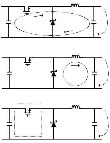 Figure 20. Typical Current Flow in a Buck Converter
10.2 Layout Example
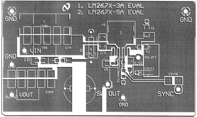 Figure 21. Top Layer Foil Pattern of Printed-Circuit Board
11 デバイスおよびドキュメントのサポート
11.1 関連資料
関連資料については、以下を参照してください。
- 『AN-1187 リードレス・リードフレーム・パッケージ(LLP)』(SNOA401)
- 『AN-1229 SIMPLE SWITCHER® PCBレイアウト・ガイドライン』(SNVA054)
11.2 ドキュメントの更新通知を受け取る方法
ドキュメントの更新についての通知を受け取るには、ti.comのデバイス製品フォルダを開いてください。右上の隅にある「通知を受け取る」をクリックして登録すると、変更されたすべての製品情報に関するダイジェストを毎週受け取れます。変更の詳細については、修正されたドキュメントに含まれている改訂履歴をご覧ください。
11.3 コミュニティ・リソース
The following links connect to TI community resources. Linked contents are provided "AS IS" by the respective contributors. They do not constitute TI specifications and do not necessarily reflect TI's views; see TI's Terms of Use.
-
TI E2E™ Online Community TI's Engineer-to-Engineer (E2E) Community. Created to foster collaboration among engineers. At e2e.ti.com, you can ask questions, share knowledge, explore ideas and help solve problems with fellow engineers.
-
Design Support TI's Design Support Quickly find helpful E2E forums along with design support tools and contact information for technical support.
11.4 商標
E2E is a trademark of Texas Instruments.
SIMPLE SWITCHER is a registered trademark of Texas Instruments.
All other trademarks are the property of their respective owners.
11.5 静電気放電に関する注意事項

これらのデバイスは、限定的なESD(静電破壊)保護機能を内 蔵しています。保存時または取り扱い時は、MOSゲートに対す る静電破壊を防止するために、リード線同士をショートさせて おくか、デバイスを導電フォームに入れる必要があります。
11.6 Glossary
SLYZ022 — TI Glossary.
This glossary lists and explains terms, acronyms, and definitions.
12 メカニカル、パッケージ、および注文情報
以降のページには、メカニカル、パッケージ、および注文に関する情報が記載されています。これらの情報は、指定のデバイスに対して提供されている最新のデータです。このデータは予告なく変更されることがあり、ドキュメントが改訂される場合もあります。本データシートのブラウザ版を使用されている場合は、画面左側の説明をご覧ください。
12.1 DAP (VSONパッケージ)
プリント基板のグランド・プレーンまたはアイランドには、ダイ取り付けパッド(DAP)を接続でき、接続する必要があります。CADおよび組み立てのガイドラインについては、アプリケーション・ノートAN1187(www.ti.com/lsds/ti/analog/powermanagement/power_portal.page)を参照してください。
IMPORTANT NOTICE
Texas Instruments Incorporated and its subsidiaries (TI) reserve the right to make corrections, enhancements, improvements and other changes to its semiconductor products and services per JESD46, latest issue, and to discontinue any product or service per JESD48, latest issue. Buyers should obtain the latest relevant information before placing orders and should verify that such information is current and complete. All semiconductor products (also referred to herein as "components") are sold subject to TI's terms and conditions of sale supplied at the time of order acknowledgment.
TI warrants performance of its components to the specifications applicable at the time of sale, in accordance with the warranty in TI's terms and conditions of sale of semiconductor products. Testing and other quality control techniques are used to the extent TI deems necessary to support this warranty. Except where mandated by applicable law, testing of all parameters of each component is not necessarily performed.
TI assumes no liability for applications assistance or the design of Buyers' products. Buyers are responsible for their products and applications using TI components. To minimize the risks associated with Buyers' products and applications, Buyers should provide adequate design and operating safeguards.
TI does not warrant or represent that any license, either express or implied, is granted under any patent right, copyright, mask work right, or other intellectual property right relating to any combination, machine, or process in which TI components or services are used. Information published by TI regarding third-party products or services does not constitute a license to use such products or services or a warranty or endorsement thereof. Use of such information may require a license from a third party under the patents or other intellectual property of the third party, or a license from TI under the patents or other intellectual property of TI.
Reproduction of significant portions of TI information in TI data books or data sheets is permissible only if reproduction is without alteration and is accompanied by all associated warranties, conditions, limitations, and notices. TI is not responsible or liable for such altered documentation. Information of third parties may be subject to additional restrictions.
Resale of TI components or services with statements different from or beyond the parameters stated by TI for that component or service voids all express and any implied warranties for the associated TI component or service and is an unfair and deceptive business practice. TI is not responsible or liable for any such statements.
Buyer acknowledges and agrees that it is solely responsible for compliance with all legal, regulatory and safety-related requirements concerning its products, and any use of TI components in its applications, notwithstanding any applications-related information or support that may be provided by TI. Buyer represents and agrees that it has all the necessary expertise to create and implement safeguards which anticipate dangerous consequences of failures, monitor failures and their consequences, lessen the likelihood of failures that might cause harm and take appropriate remedial actions. Buyer will fully indemnify TI and its representatives against any damages arising out of the use of any TI components in safety-critical applications.
In some cases, TI components may be promoted specifically to facilitate safety-related applications. With such components, TI's goal is to help enable customers to design and create their own end-product solutions that meet applicable functional safety standards and requirements. Nonetheless, such components are subject to these terms.
No TI components are authorized for use in FDA Class III (or similar life-critical medical equipment) unless authorized officers of the parties have executed a special agreement specifically governing such use.
Only those TI components which TI has specifically designated as military grade or "enhanced plastic" are designed and intended for use in military/aerospace applications or environments. Buyer acknowledges and agrees that any military or aerospace use of TI components which have not been so designated is solely at the Buyer's risk, and that Buyer is solely responsible for compliance with all legal and regulatory requirements in connection with such use.
TI has specifically designated certain components as meeting ISO/TS16949 requirements, mainly for automotive use. In any case of use of non-designated products, TI will not be responsible for any failure to meet ISO/TS16949.
Products
- Audio: www.ti.com/audio
- Amplifiers: amplifier.ti.com
- Data Converters: dataconverter.ti.com
- DLP® Products: www.dlp.com
- DSP: dsp.ti.com
- Clocks and Timers: www.ti.com/clocks
- Interface: interface.ti.com
- Logic: logic.ti.com
- Power Mgmt: power.ti.com
- Microcontrollers: microcontroller.ti.com
- RFID: www.ti.rfid.com
- OMAP Application Processors: www.ti.com/omap
- Wireless Connectivity: www.ti.com/wirelessconnectivity
Applications
- Automotive and Transportation: www.ti.com/automotive
- Communications and Telecom: www.ti.com/communications
- Computers and Peripherals: www.ti.com/computers
- Consumer Electronics: www.ti.com/consumer-apps
- Energy and Lighting: www.ti.com/energy
- Industrial: www.ti.com/industrial
- Medical: www.ti.com/medical
- Security: www.ti.com/security
- Space, Avionics and Defense: www.ti.com/space-avionics-defense
- Video & Imaging: www.ti.com/video
TI E2E Community : e2e.ti.com
Mailing Address: Texas Instruments, Post Office Box 655303, Dallas, Texas 75265
Copyright© 2016, Texas Instruments Incorporated