SNIS144G July 2007 – September 2016 LM26LV , LM26LV-Q1
PRODUCTION DATA.
- 1 Features
- 2 Applications
- 3 Description
- 4 Revision History
- 5 Pin Configuration and Functions
- 6 Specifications
-
7 Detailed Description
- 7.1 Overview
- 7.2 Functional Block Diagram
- 7.3 Feature Description
- 7.4 Device Functional Modes
- 8 Application and Implementation
- 9 Power Supply Recommendations
- 10Layout
- 11Device and Documentation Support
- 12Mechanical, Packaging, and Orderable Information
1 Features
- Low 1.6-V Operation
- Low Quiescent Current
- Latching Function: Device Can Latch the Over Temperature Condition
- Push-Pull and Open-Drain Temperature Switch Outputs
- Wide Trip Point Range of 0°C to 150°C
- Very Linear Analog VTEMP Temperature Sensor Output
- VTEMP Output Short-Circuit Protected
- Accurate Over –50°C to 150°C Temperature Range
- Excellent Power Supply Noise Rejection
- LM26LVQISD-130 and LM26LVQISD-135 are AEC-Q100 Qualified and are Manufactured on an Automotive Grade Flow:
- Device Temperature Grade 0: –40°C to 150°C Ambient Operating Temperature Range
- Device HBM ESD Classification Level 3 A
- Device CDM ESD Classification Level C6
- Device MM ESD Classification Level M3
2 Applications
- Cell Phones and Wireless Transceivers
- Digital Cameras
- Battery Management Systems
- Automotive Applications
- Disk Drives
- Games and Appliances
3 Description
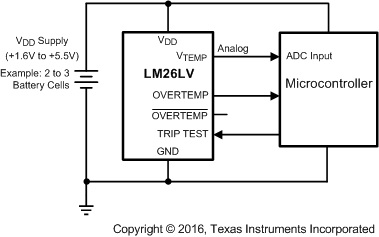
The LM26LV and LM26LV-Q1 are low-voltage, precision, dual-output, low-power temperature switches and temperature sensors. The temperature trip point (TTRIP) can be preset at the factory to any temperature in the range of 0°C to 150°C in 1°C increments. Built-in temperature hysteresis (THYST) keeps the output stable in an environment of temperature instability.
In normal operation the LM26LV or LM26LV-Q1 temperature switch outputs assert when the die temperature exceeds TTRIP. The temperature switch outputs will reset when the temperature falls below a temperature equal to (TTRIP – THYST). The OVERTEMP digital output, is active-high with a push-pull structure, while the OVERTEMP digital output, is active-low with an open-drain structure.
The analog output, VTEMP, delivers an analog output voltage with Negative Temperature Coefficient (NTC).
Driving the TRIP_TEST input high causes the digital outputs to be asserted for in-situ verification and causes the threshold voltage to appear at the VTEMP output pin, which could be used to verify the temperature trip point.
The LM26LV's and LM26LV-Q1's low minimum supply voltage makes them ideal for 1.8-V system designs. The wide operating range, low supply current, and excellent accuracy provide a temperature switch solution for a wide range of commercial and industrial applications.
Device Information(1)
| PART NUMBER | PACKAGE | BODY SIZE (NOM) |
|---|---|---|
| LM26LV, LM26LV-Q1 | WSON (6) | 2.20 mm × 2.50 mm |
- For all available packages, see the orderable addendum at the end of the data sheet.
Redundant Protection and Monitoring

Typical Transfer Characteristic
