SNIS144G July 2007 – September 2016 LM26LV , LM26LV-Q1
PRODUCTION DATA.
- 1 Features
- 2 Applications
- 3 Description
- 4 Revision History
- 5 Pin Configuration and Functions
- 6 Specifications
-
7 Detailed Description
- 7.1 Overview
- 7.2 Functional Block Diagram
- 7.3 Feature Description
- 7.4 Device Functional Modes
- 8 Application and Implementation
- 9 Power Supply Recommendations
- 10Layout
- 11Device and Documentation Support
- 12Mechanical, Packaging, and Orderable Information
8 Application and Implementation
NOTE
Information in the following applications sections is not part of the TI component specification, and TI does not warrant its accuracy or completeness. TI’s customers are responsible for determining suitability of components for their purposes. Customers should validate and test their design implementation to confirm system functionality.
8.1 Application Information
8.1.1 ADC Input Considerations
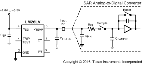
The LM26LV and LM26LV-Q1 have an analog temperature sensor output VTEMP that can be directly connected to an ADC (Analog-to-Digital Converter) input. Most CMOS ADCs found in microcontrollers and ASICs have a sampled data comparator input structure. When the ADC charges the sampling cap, it requires instantaneous charge from the output of the analog source such as the LM26LV or LM26LV-Q1 temperature sensor. This requirement is easily accommodated by the addition of a capacitor (CFILTER). The size of CFILTER depends on the size of the sampling capacitor and the sampling frequency. Because not all ADCs have identical input stages, the charge requirements vary. This general ADC application is shown as an example only.
 Figure 26. Suggested Connection to a Sampling Analog-to-Digital Converter Input Stage
8.2 Typical Application
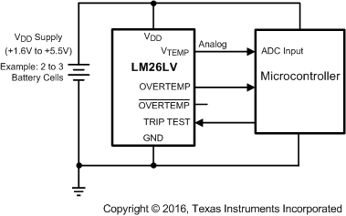
 Figure 27. Typical Application Schematic
8.2.1 Design Requirements
For this design example, use the parameters listed in Table 3 as the input parameters.
Table 3. Design Parameters
| PARAMETER | EXAMPLE VALUE |
|---|---|
| Temperature | 0°C to 150°C (LM26LV), –40°C to 85°C for microcontroller |
| Accuracy | ±2.3°C (Gain1, TA = 0°C to 150°C) |
| VDD | 3.3 V |
| IDD | 8 µA |
8.2.2 Detailed Design Procedure
The LM26LV and LM26LV-Q1 come with a factory preset trip point. See Mechanical, Packaging, and Orderable Information for available trip point options. Figure 27 shows the device's OVERTEMP output driving a microcontroller interrupt input to indicate an overtemperature event. In addition to the OVERTEMP output, a OVERTEMP output is available for use depending on the interrupt polarity of the microcontroller's interrupt pin. A VTEMP analog output is available to drive the microcontroller ADC input allowing the microcontroller to determine the sensing temperature of the LM26LV or LM26LV-Q1. The TRIP_TEST input is connected to a microcontroller output pin allowing the microcontroller to run on the fly electrical conductivity testing. For normal operation TRIP_TEST must be driven low by the microcontroller output. If no testing is required, the TRIP_TEST pin may be continuously grounded.
8.2.3 Application Curves
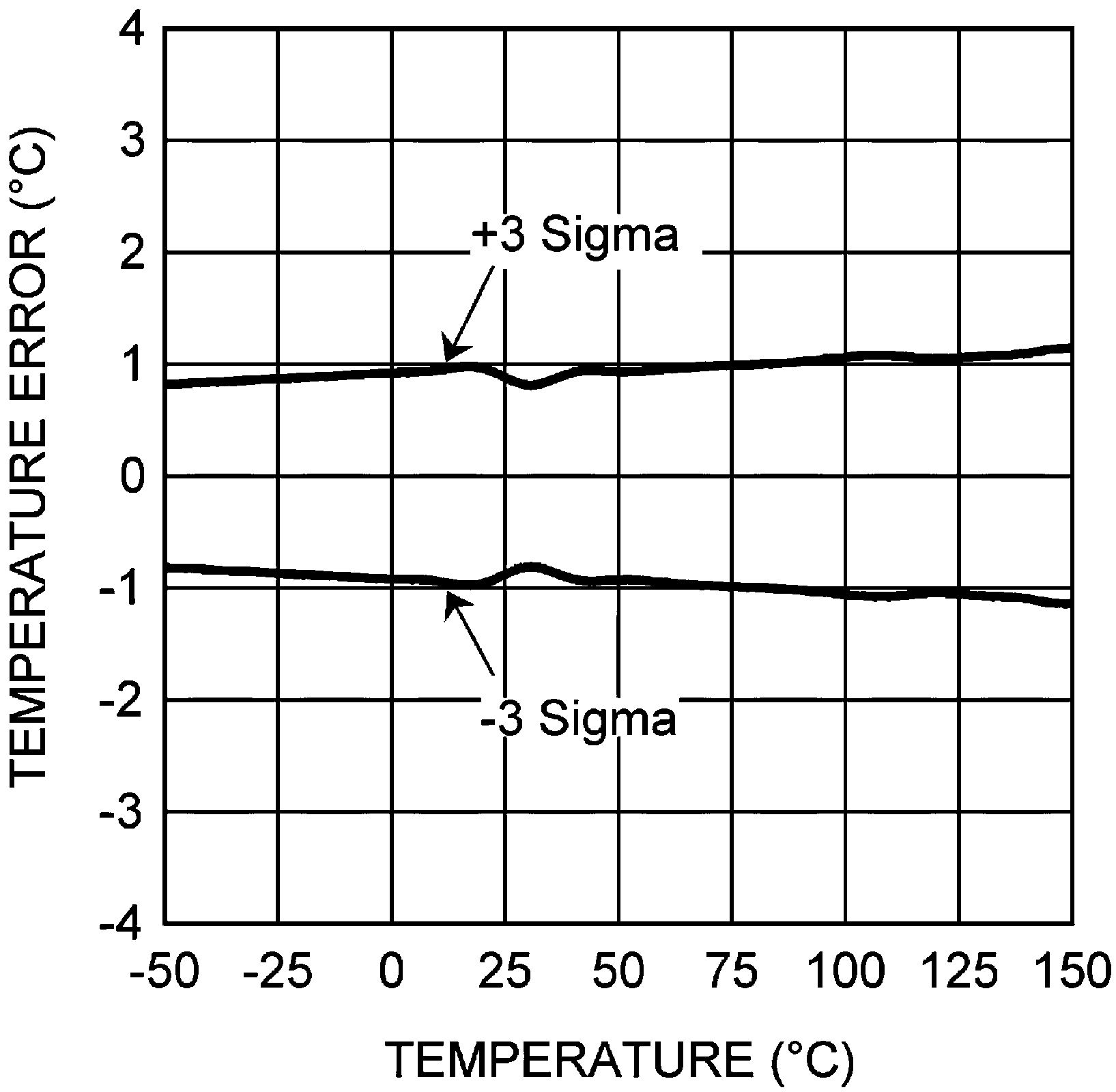
 Figure 28. VTEMP Analog Output Temperature Error
 Figure 29. Switch Output Function