JAJSG39 September 2018 LM2735-Q1
PRODUCTION DATA.
- 1 特長
- 2 アプリケーション
- 3 概要
- 4 改訂履歴
- 5 Pin Configuration and Functions
- 6 Specifications
- 7 Detailed Description
-
8 Application and Implementation
- 8.1 Application Information
- 8.2
Typical Applications
- 8.2.1 LM2735X-Q1 SOT-23 Design Example 1
- 8.2.2 LM2735Y-Q1 SOT-23 Design Example 2
- 8.2.3 LM2735X-Q1 WSON Design Example 3
- 8.2.4 LM2735Y-Q1 WSON Design Example 4
- 8.2.5 LM2735X-Q1 SOT-23 Design Example 6
- 8.2.6 LM2735Y-Q1 SOT-23 Design Example 7
- 8.2.7 LM2735X-Q1 SOT-23 Design Example 8
- 8.2.8 LM2735Y-Q1 SOT-23 Design Example 9
- 8.2.9 LM2735X-Q1 WSON Design Example 10
- 8.2.10 LM2735Y-Q1 WSON Design Example 11
- 8.2.11 LM2735X-Q1 WSON SEPIC Design Example 12
- 8.2.12 LM2735X-Q1 SOT-23 LED Design Example 14
- 8.2.13 LM2735Y-Q1 WSON FlyBack Design Example 15
- 8.2.14 LM2735X-Q1 SOT-23 LED Design Example 16 VRAIL > 5.5 V Application
- 8.2.15 LM2735X-Q1 SOT-23 LED Design Example 17 Two-Input Voltage Rail Application
- 8.2.16 SEPIC Converter
- 9 Power Supply Recommendations
- 10Layout
- 11デバイスおよびドキュメントのサポート
- 12メカニカル、パッケージ、および注文情報
7.3.4 Compensation
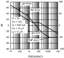
The LM2735-Q1 uses constant-frequency peak current mode control. This mode of control allows for a simple external compensation scheme that can be optimized for each application. A complicated mathematical analysis can be completed to fully explain the internal and external compensation of the LM2735-Q1, but for simplicity, a graphical approach with simple equations will be used. Below is a Gain and Phase plot of a LM2735-Q1 that produces a 12-V output from a 5-V input voltage. The Bode plot shows the total loop Gain and Phase without external compensation.
 Figure 15. LM2735-Q1 Without External Compensation
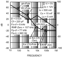
 One can see that the crossover frequency is fine, but the phase margin at 0 dB is very low (22°). A zero can be placed just above the crossover frequency so that the phase margin will be bumped up to a minimum of 45°. Below is the same application with a zero added at 8 kHz.
 Figure 16. LM2735-Q1 With External Compensation
 The simplest method to determine the compensation component value is as follows.
Set the output voltage with Equation 1.

where
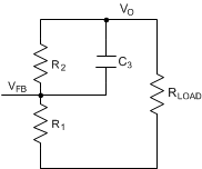
- R1 is the bottom resistor and R2 is the resistor tied to the output voltage.
The next step is to calculate the value of C3. The internal compensation has been designed so that when a zero is added from 5 kHz to 10 kHz, the converter will have good transient response with plenty of phase margin for all input and output voltage combinations.

Lower output voltages will have the zero set closer to 10 kHz, and higher output voltages will usually have the zero set closer to 5 kHz. TI recommends obtaining a gain and phase plot for your actual application. See Application and Implementation to obtain examples of working applications and the associated component values.
Pole at origin due to internal GM amplifier:
Pole due to output load and capacitor:

Equation 4 only determines the frequency of the pole for perfect current mode control (CMC). That is, it doesn’t take into account the additional internal artificial ramp that is added to the current signal for stability reasons. Adding artificial ramp begins to move away from CMC to voltage mode control (VMC). The artifact is that the pole due to the output load, and output capacitor is actually slightly higher in frequency than calculated. In this example, it is calculated at 650 Hz, but in reality, it is around 1 kHz.
The zero created with capacitor C3 and resistor R2:
 Figure 17. Setting External Pole-Zero
There is an associated pole with the zero that was created in Equation 5.

It is always higher in frequency than the zero.
A right-half plane zero (RHPZ) is inherent to all boost converters. One must remember that the gain associated with a right-half plane zero increases at 20 dB per decade, but the phase decreases by 45° per decade. For most applications there is little concern with the RHPZ due to the fact that the frequency at which it shows up is well beyond crossover and has little to no effect on loop stability. One must be concerned with this condition for large inductor values and high output currents.

There are miscellaneous poles and zeros associated with parasitics internal to the LM2735-Q1, external components, and the PCB. They are located well over the crossover frequency, and for simplicity are not discussed.