JAJSG39 September 2018 LM2735-Q1
PRODUCTION DATA.
- 1 特長
- 2 アプリケーション
- 3 概要
- 4 改訂履歴
- 5 Pin Configuration and Functions
- 6 Specifications
- 7 Detailed Description
-
8 Application and Implementation
- 8.1 Application Information
- 8.2
Typical Applications
- 8.2.1 LM2735X-Q1 SOT-23 Design Example 1
- 8.2.2 LM2735Y-Q1 SOT-23 Design Example 2
- 8.2.3 LM2735X-Q1 WSON Design Example 3
- 8.2.4 LM2735Y-Q1 WSON Design Example 4
- 8.2.5 LM2735X-Q1 SOT-23 Design Example 6
- 8.2.6 LM2735Y-Q1 SOT-23 Design Example 7
- 8.2.7 LM2735X-Q1 SOT-23 Design Example 8
- 8.2.8 LM2735Y-Q1 SOT-23 Design Example 9
- 8.2.9 LM2735X-Q1 WSON Design Example 10
- 8.2.10 LM2735Y-Q1 WSON Design Example 11
- 8.2.11 LM2735X-Q1 WSON SEPIC Design Example 12
- 8.2.12 LM2735X-Q1 SOT-23 LED Design Example 14
- 8.2.13 LM2735Y-Q1 WSON FlyBack Design Example 15
- 8.2.14 LM2735X-Q1 SOT-23 LED Design Example 16 VRAIL > 5.5 V Application
- 8.2.15 LM2735X-Q1 SOT-23 LED Design Example 17 Two-Input Voltage Rail Application
- 8.2.16 SEPIC Converter
- 9 Power Supply Recommendations
- 10Layout
- 11デバイスおよびドキュメントのサポート
- 12メカニカル、パッケージ、および注文情報
5 Pin Configuration and Functions
DBV Package
5-Pin SOT-23
Top View

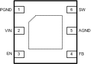
NGG Package
6-Pin WSON
Top View

Pin Functions
| PIN | I/O | DESCRIPTION | ||
|---|---|---|---|---|
| NAME | SOT-23 | WSON | ||
| AGND | — | 5 | PWR | Signal ground pin. Place the bottom resistor of the feedback network as close as possible to this pin and pin 4. |
| EN | 4 | 3 | I | Shutdown control input. Logic high enables operation. Do not allow this pin to float or be greater than VIN + 0.3 V. |
| FB | 3 | 4 | I | Feedback pin. Connect FB to external resistor-divider to set output voltage. |
| GND | 2 | DAP | PWR | Signal and power ground pin. Place the bottom resistor of the feedback network as close as possible to this pin.
For WSON, connect to pin 1 and pin 5 on top layer. Place 4-6 vias from DAP to bottom layer GND plane. |
| NC | — | — | — | No Connect |
| PGND | — | 1 | PWR | Power ground pin. Place PGND and output capacitor GND close together. |
| SW | 1 | 6 | O | Output switch. Connect to the inductor, output diode. |
| VIN | 5 | 2 | PWR | Supply voltage for power stage, and input supply voltage. |