SNVS896B August 2013 – November 2014 LM27403
PRODUCTION DATA.
- 1 Features
- 2 Applications
- 3 Description
- 4 Revision History
- 5 Description (Continued)
- 6 Pin Configuration and Functions
- 7 Specifications
-
8 Detailed Description
- 8.1 Overview
- 8.2 Functional Block Diagram
- 8.3
Feature Description
- 8.3.1 Input Range: VIN
- 8.3.2 Output Voltage: FB Voltage and Accuracy
- 8.3.3 Input and Bias Rail Voltages: VIN and VDD
- 8.3.4 Precision Enable: UVLO/EN
- 8.3.5 Switching Frequency
- 8.3.6 Temperature Sensing: D+ and D-
- 8.3.7 Thermal Shutdown: OTP
- 8.3.8 Inductor-DCR-Based Overcurrent Protection
- 8.3.9 Current Sensing: CS+ and CS-
- 8.3.10 Current Limit Handling
- 8.3.11 Soft-Start: SS/TRACK
- 8.3.12 Monotonic Startup
- 8.3.13 Prebias Startup
- 8.3.14 Voltage-Mode Control
- 8.3.15 Output Voltage Remote Sense: RS
- 8.3.16 Power Good: PGOOD
- 8.3.17 Gate Drivers: LG and HG
- 8.3.18 Sink and Source Capability
- 8.4 Device Functional Modes
-
9 Application and Implementation
- 9.1 Application Information
- 9.2
Typical Applications
- 9.2.1 Design 1 - High-Efficiency Synchronous Buck Regulator for Telecom Power
- 9.2.2 Design 2 - Powering FPGAs Using Flexible 30A Regulator With Small Footprint
- 9.2.3 Design 3 - Powering Multicore DSPs
- 9.2.4 Design 4 - Regulated 12-V Rail with LDO Low-Noise Auxiliary Output for RF Power
- 9.2.5 Design 5 - High Power Density Implementation From 3.3-V or 5-V Supply Rail
- 10Power Supply Recommendations
- 11Layout
- 12Device and Documentation Support
- 13Mechanical, Packaging, and Orderable Information
パッケージ・オプション
メカニカル・データ(パッケージ|ピン)
- RTW|24
サーマルパッド・メカニカル・データ
- RTW|24
発注情報
8 Detailed Description
8.1 Overview
The distributed power supply architecture, pervasive in myriad applications including communications infrastructure equipment and computing systems, uses an intermediate bus and multiple downstream DC-DC regulators dedicated and proximate to each “point-of-load.” The ASICs, FPGAs, and microprocessors that comprise these loads have supply voltage requirements whose levels are decreasing on an absolute basis and whose tolerance bands are decreasing on a percentage basis. The hallmarks of point-of-load (POL) DC-DC regulators are efficiency, size, load transient response, and cost.
To this end, the LM27403 is a feature-rich, easy-to-use, synchronous PWM DC-DC step-down controller capable of providing an ultrahigh current output for demanding, high power density POL applications. An input voltage range of 3 V to 20 V is compatible with a wide range of intermediate bus system rails and battery chemistries; especially 3.3-V, 5-V, and 12-V inputs. The output voltage is adjustable from 0.6 V to as high as 93% of the input voltage, with better than ±1% feedback system regulation accuracy over the full junction temperature range. With an accurate, adjustable and thermally compensated inductor DCR based current limit setpoint, ferrite and composite core inductors with low DCR and small footprint can be specified to maximize efficiency and reduce power loss. High-current gate drivers with adaptive deadtime are used for the high-side and low-side MOSFETs to provide further efficiency gains.
The LM27403 employs a voltage-mode control loop with output voltage remote sense, input voltage feedforward modulation, and a high gain-bandwidth error amplifier to accurately regulate the output voltage over substantial load, line, and temperature ranges. The switching frequency is programmable between 200 kHz and 1.2 MHz through a resistor or an external synchronization signal. The LM27403 is available in a 4-mm × 4-mm, thermally enhanced, 24-lead WQFN PowerPad package. This device offers high levels of integration by including MOSFET gate drivers, a low dropout (LDO) bias supply linear regulator, and comprehensive fault protection features to enable highly flexible, reliable, energy-efficient, and high power density regulator solutions.
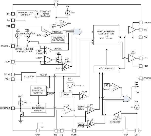
Multiple fault conditions are accommodated, including overvoltage, undervoltage, overcurrent, and overtemperature. To improve overcurrent setpoint accuracy and enable easier filter inductor selection, the LM27403 thermally compensates for the temperature coefficient (TC) of the inductor's winding resistance by sensing the inductor temperature with an external NPN transistor configured as a thermal diode. The same thermal diode also monitors the PCB temperature to initiate a thermal shutdown in the event that the sensed temperature exceeds the programmed thermal shutdown setpoint.
8.2 Functional Block Diagram
8.3 Feature Description
8.3.1 Input Range: VIN
The LM27403 operational input voltage range is from 3 V to 20 V. The device is intended for POL conversions from 3.3-V, 5-V, and 12-V unregulated, semiregulated and fully regulated supply rails. It is also suitable for connection to intermediate bus converters with output rails centered at 12 V and 9.6 V (derived from 4:1 and 5:1 primary-secondary transformer step-downs in nonregulated full-bridge converter topologies) and voltage levels intrinsic to a wide variety of battery chemistries.
The LM27403 uses an internal LDO subregulator to provide a 4.7-V bias rail for the gate drive and control circuits (assuming the input voltage is higher than 4.7 V plus the necessary subregulator dropout specification). Naturally, it can be more favorable to connect VDD directly to the input during low input voltage operation (VVIN < 5.5 V). In summary, connecting VDD to VIN during low input voltage operation provides a greater gate drive voltage level and thus an inherent efficiency benefit. However, by virtue of the low subregulator dropout voltage, this VDD to VIN connection is not mandatory, thus enabling input ranges from 3 V up to 20 V. The application circuits shown below detail LM27403 configuration options suitable for several input rails.
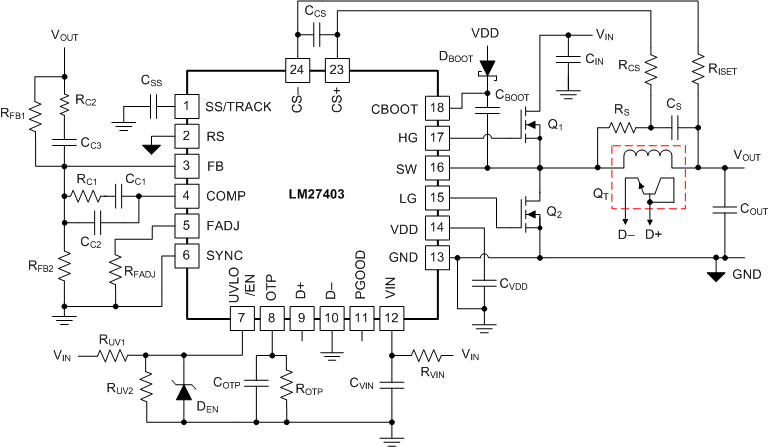 Figure 23. Schematic Diagram for VIN Operating Range of 3 V to 20 V
Figure 23 shows the schematic diagram for an input voltage ranging from 3 V to 20 V. Note that a finite subregulator dropout voltage exists and is manifested to a larger extent when driving high gate charge (QG) power MOSFETs at elevated switching frequencies. For example, at VVIN = 3 V, the VDD rail voltage is 2.8 V with a dc operating current, IVDD, of 40 mA. Such a low gate drive rail may be insufficient to fully enhance the power MOSFET gates. At the very least, MOSFET on-state resistance, RDS(ON), increases at such low gate drive levels. Here are the main concerns when operating at a low input voltage:
- Increase of conduction losses (higher RDS(on) at lower VGS).
- Increase of switching losses associated with sluggish switching times when operating at low VGS levels.
- Deadtime may be larger as a result of the lower gate drive level and associated slower gate voltage slew rate. This may become evident, for example, when using two high-side MOSFETs in a 3.3-V to 2.5-V converter design.
- Dramatic reduction in the range of suitable MOSFETs that a designer can choose from (MOSFETs with RDS(on) rated at VGS = 2.5 V become mandatory).
Note that the increased on-state resistance is compounded by an increase in MOSFET junction temperature, bearing in mind the negative temperature coefficient of the MOSFET threshold voltage.
In general, the subregulator is rated to drive the two internal gate driver stages in addition to the quiescent current associated with LM27403 operation. Figure 24 shows the schematic diagram for lower input voltages such as 3.0 V to 5.5 V. The LM27403's VDD and VIN pins can be tied together if the input voltage is guaranteed not to exceed 5.5 V (absolute maximum 6 V). This short bypasses the internal LDO bias regulator and eliminates the LDO dropout voltage and power dissipation. An RC filter from the input rail to the VIN pin, for example 2.2 Ω and 1 µF, presents supplementary filtering at the VIN pin. Low gate threshold voltage MOSFETs are recommended for this configuration.
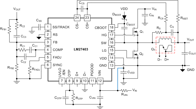 Figure 24. Schematic Diagram for VIN Operating Range of 3.0 V to 5.5 V
8.3.2 Output Voltage: FB Voltage and Accuracy
The reference voltage seen at the FB pin is set at 0.6 V, and a feedback system accuracy of ±1% over the full junction temperature range is met. Junction temperature range for the device is –40°C to +125°C. While somewhat dependent on frequency and load current levels, the LM27403 is generally capable of providing output voltages in the range of 0.6 V to a maximum of greater than 90% VIN. The dc output voltage during normal operation is set by the feedback resistor network, RFB1 and RFB2, connected to VOUT.
8.3.3 Input and Bias Rail Voltages: VIN and VDD
The LM27403 internal UVLOs ensure that the input rail (VIN) and bias supply rail (VDD) are charged and stable at 2.7 V before switching begins. VDD and VIN have independent UVLO comparators, each with 250 mV of hysteresis. There is a definite delay between UVLO power-on and switching power-on. This delay is related to the fact that the LM27403 does not begin switching until the internal temperature sense circuitry is ready and stabilized. The delay is four measurement cycles on D+, equivalent to 512 clock cycles.
The VDD bias supply LDO has a nominal current limit of 106 mA during normal operation. However, a lower current limit is engaged at startup to control the rate of rise of the VDD voltage. Figure 25 shows the typical scope waveforms of VDD and VOUT when the input voltage is instantaneously applied. Here, the VDD voltage ramps in approximately 1.4 ms based on a 10-µF VDD decoupling capacitor and current-limited VDD feature. For more details, please see the LM27403 EVM User's Guide, SNVU233.
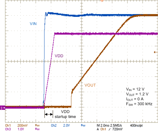 Figure 25. Typical Startup Waveforms of VDD and VOUT With Controlled Ramp Rates
8.3.4 Precision Enable: UVLO/EN
The UVLO/EN pin represents a precision analog enable function for user-defined UVLO power-on input voltage levels and to toggle the output on and off. The UVLO/EN pin is essentially a comparator-based input referenced to a flat bandgap voltage with a fixed hysteresis of 165 mV.
The UVLO/EN pin has an internal pullup current of 1.8 µA, as shown in Figure 26. There is also a low IQ shutdown mode when UVLO/EN is effectively pulled below a base-emitter voltage drop (approximately 0.7 V at room temperature). This mode shuts down the bias currents of the LM27403, but the UVLO/EN pullup current source is still available. If UVLO/EN is pulled below this hard shutdown threshold, the internal LDO regulator powers off and the VDD rail collapses.
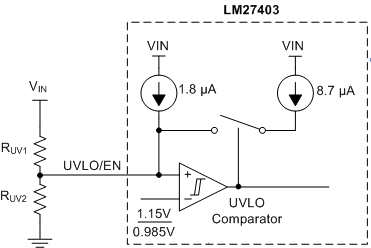 Figure 26. Precision UVLO/Enable Circuit with Hysteretic Comparator and Pullup Current Sources
When the precision enable threshold of 1.15 V is exceeded, the UVLO/EN pullup current source increases from 1.8 µA to 10.5 µA (that is, an 8.7-µA hysteresis current). Use this feature to create a customizable UVLO hysteresis (above the standard 165-mV fixed voltage hysteresis) based on the resistor divider from VIN to turn on and off the LM27403 at the required input voltage levels. Also, use a capacitor from the UVLO/EN pin to GND to implement a fixed time delay in power systems with timed sequencing requirements.
Figure 27 shows an example using the circuit in Figure 23 where the input voltage is ramping from 0 V to 10 V in 100 ms. Here, the UVLO resistors, RUV1 and RUV2, are respectively set to 47.5 kΩ and 10 kΩ. Given these resistances, the typical input UVLO turn-on and turn-off levels are 6.5 V and 5.2 V, respectively. The UVLO/EN pin voltage steps at the rising and falling thresholds are defined by the UVLO/EN pin current hysteresis.
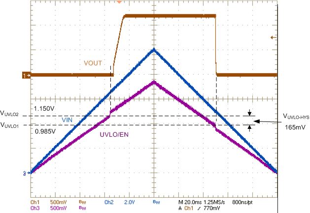 Figure 27. Typical Input Voltage UVLO Turn On and Off Behavior
Given VIN(on) and VIN(off) as the input voltage turn-on and turn-off thresholds, respectively, select the UVLO resistors using the following expressions:


The UVLO/EN pin has a maximum operating voltage rating equal to the input voltage or 5.5V, whichever is lower. Do not exceed this rating. If the input UVLO level is set at low input voltage, it is possible that this maximum UVLO/EN pin voltage could be exceeded at the higher end of the input voltage operating range. In this case, use a small 4.7-V zener diode clamp, designated DEN in Figure 23, from UVLO/EN to GND, such that the maximum operating level is never exceeded.
8.3.5 Switching Frequency
There are two options for setting the switching frequency of the LM27403, thus providing a power supply designer a level of flexibility when choosing external components for multiple applications. To adjust the frequency, use a resistor from the FADJ pin to GND, or synchronize the LM27403 to an external clock signal through the SYNC pin.
8.3.5.1 Frequency Adjust: FADJ
Adjust the LM27403 free-running switching frequency by using a resistor from the FADJ pin to GND. The switching frequency range of the device is from 200 kHz to 1.2 MHz. An open circuit at the FADJ pin forces the frequency to the minimum value. FADJ shorted moves the frequency to its maximum value. The frequency set resistance, RFADJ, is governed by Equation 3.

E96 resistors for common switching frequencies are given in Table 1.
Table 1. Frequency Set Resistors
| SWITCHING FREQUENCY (kHz) | FREQUENCY SET RESISTANCE (kΩ) |
|---|---|
| 215 | 95.3 |
| 250 | 68.1 |
| 300 | 47.5 |
| 500 | 20 |
| 600 | 15 |
| 800 | 7.5 |
| 1050 | 4.12 |
| 1200 | 2.87 |
8.3.5.2 Clock Synchronization: SYNC
Apply an external clock synchronization signal to the LM27403 to synchronize switching in both frequency and phase. Requirements for the clock SYNC signal are:
- Clock SYNC range: 200 kHz to 1.2 MHz
- SYNC frequency range from the FADJ frequency: up to 400 kHz (up only)
Figure 28 shows a SYNC TTL signal at 600 kHz and the corresponding SW node waveform (VIN = 12 V, VOUT = 1.2 V, free-running frequency = 250 kHz). The synchronization is with respect to the rising edge of SYNC. The rising edge of the SW voltage is phase delayed relative to SYNC by approximately 250 ns.
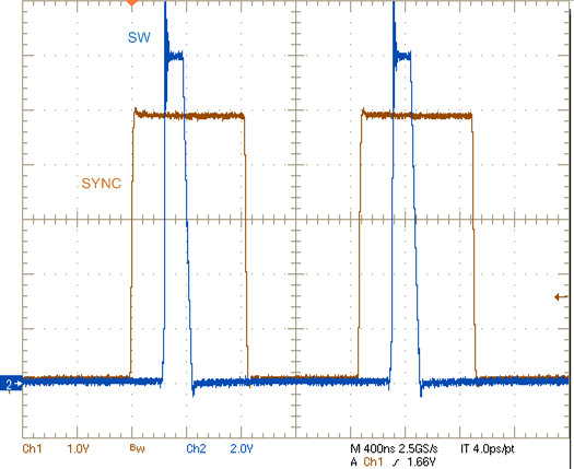 Figure 28. Typical 600-kHz SYNC Waveform
8.3.6 Temperature Sensing: D+ and D–
The LM27403 PWM controller offers low-cost programmable thermal protection by using remote thermal diode temperature measurements based on the change in forward bias voltage of a diode when operated at two different currents. The thermal diode is a discrete small-signal 2N3904 type silicon NPN BJT located (in good thermal contact) adjacent the filter inductor.
The ideality factor is a parameter in the diode I-V relationship that approaches 1.0 or 2.0 as carrier diffusion or recombination current dominate current flow, respectively. The ideality factor for 2N3904 type diode-connected BJTs available from several manufacturers is typically 1.004. Note that 3-terminal BJTs such as the 2N3904 are vastly preferred over true 2-terminal diodes in this application. Discrete 2-terminal diodes with current largely dictated by recombination have a much higher ideality factor (η = 1.2 to 1.5) than BJTs and, to such an extent, would cause unacceptable temperature measurement error.
Switched capacitor technology is integrated in the LM27403 to sample and measure the base-emitter voltages created by respective 10-µA and 100-µA bias currents flowing from the D+ to D– pins. The difference in these voltages, termed ΔVBE, is readily extracted and the sensed temperature is calculated noting that ΔVBE is directly proportional to temperature as follows:

where
- k = Boltzmann’s constant, 1.3806488 × 10⁻²³J/K (Joules/Kelvin)
- T = absolute temperature in Kelvin (K)
- q = electron charge = 1.602176 x 10⁻¹⁹ C (Coulombs)
- η = diode ideality factor = 1.004
- Ilow = bias current in state 1 = 10 µA
- Ihigh = bias current in state 2 = 100 µA
The source currents from the D+ pin during state 1 and state 2 are 10 µA and 100 µA, respectively. The sensed temperature in Kelvin becomes:

Figure 29 shows the 2N3904 VBE voltage at ambient temperatures of –40°C, 25°C and 125°C. The low and high states in VBE voltage correspond to the 10-µA and 100-µA currents sourced from D+, each of 64 clock cycle duration. The voltage level is sampled at the end of each state. While the dc level of the VBE voltage decreases logarithmically with increasing temperature, the ΔVBE amplitude increases with and is directly proportional to temperature according to Equation 5.
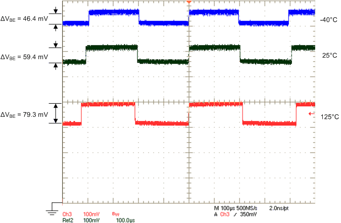 Figure 29. Typical 2N3904 Base-Emitter Voltage at –40°C, 25°C and 125°C
Note that D– is essentially a kelvin connection to the remote thermal diode. As such, the D– pin needs to be tied to GND at the LM27403; the D– trace should not connect to any of the PCBs current-carrying ground planes.
8.3.7 Thermal Shutdown: OTP
A current proportional to the sensed temperature is sourced from the OTP pin. The resultant voltage at the OTP pin (set by a resistor connected from OTP to GND) is compared to an internal shutdown threshold of 1.15 V with 80-mV hysteresis. When the threshold is exceeded, the device stops switching until the sensed temperature drops to a level where the OTP pin voltage falls to the restart threshold. The external thermal protection is disabled by grounding the OTP pin. The thermal shutdown setpoint is governed by Equation 6:

where
- ROTP is the required resistance at the OTP pin for the desired thermal shutdown temperature
- ROTP(125°C) is the nominal resistance at the OTP pin , 80.7 kΩ, for 125°C thermal shutdown, and
- TOTP is the desired thermal shutdown temperature.
For example, the OTP resistor required for a thermal shutdown setpoint of 105°C is calculated as shown in Equation 7:

A 100-nF capacitor connected in parallel with ROTP is required. When the IC detects an overtemperature event, it responds with the normal hiccup-mode sequence of events when going into shutdown. More specifically, the following steps occur when an internal or external OTP event is detected:
- The high-side MOSFET immediately turns off.
- An internal zero-cross circuit is enabled to detect whether the inductor current is positive or negative:
- If the current is negative, the low-side MOSFET immediately turns off.
- If the current is positive, the low-side MOSFET turns off when the inductor current ramps down to zero.
Note that it is important to prevent water-soluble flux residues from contaminating the PCB during the manufacturing process. Contaminants such as these can result in unexpected leakage currents and consequent temperature-measurement errors.
8.3.8 Inductor-DCR-Based Overcurrent Protection
The LM27403 exploits the filter inductor DCR to detect overcurrent events. This technique enables lossless and continuous monitoring of the output current using an RC sense network in parallel with the inductor. DCR current sensing allows the system designer to use inductors specified with low tolerance DCRs to improve the current limit setpoint accuracy. A dc current limit setpoint accuracy within the range of 10% to 15% is easily achieved using inductors with low DCR tolerances.
8.3.9 Current Sensing: CS+ and CS–
As mentioned, the LM27403 implements an inductor DCR lossless current sense scheme designed to provide both accurate overload (current limit) and short-circuit protection. Figure 30 shows the popular inductor DCR current sense method. Figure 31 shows an implementation with current shunt resistor, RISNS.
Components RS and CS in Figure 30 create a low-pass filter across the inductor to enable differential sensing of the inductor DCR voltage drop. When RSCS is equal to L/Rdcr, the voltage developed across the sense capacitor, CS, is a replica of the inductor DCR's voltage waveform. Choose the capacitance of CS greater than 0.1 µF to maintain low impedance of the sense network, thus reducing the susceptibility of noise pickup from the switch node.
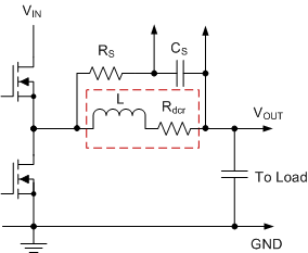 Figure 30. Current Sensing Using Inductor DCR
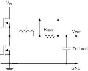 Figure 31. Current Sensing Using Shunt Resistor
The current limit circuit arrangement is portrayed in Figure 32. The current limit setpoint is set by a single external resistor, RISET, connected from the CS– pin to the output voltage terminal. The current sourced from CS– in combination with this series resistance sets the reference voltage to the current limit comparator, as governed by Equation 8.

where
- ICS is the CS– pin current, 9.9 µA typically at 25°C
- IOCP is the dc overcurrent protection setpoint, and
- ΔiL is the peak-to-peak inductor ripple current.
Inductor DCR temperature compensation is automatically provided using the remote-diode sensed temperature. The temperature coefficient (TC) of the inductor winding resistance is typically 3720 ppm/°C. The current-limit setpoint is maintained essentially constant over temperature by the slope of CS– pin current over temperature. An increase in sensed DCR voltage associated with an increase of inductor winding temperature is matched by a concomitant increase in current limit comparator reference voltage. The inductor temperature is measured by placing an external diode-connected 2N3904 discrete NPN transistor, designated QT in Figure 32, in close proximity to the inductor (see the Temperature Sensing: D+ and D– section for more details).
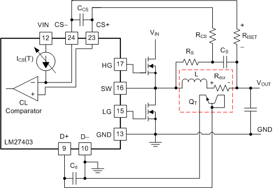 Figure 32. Current-Limit Setpoint Defined by Current Source ICS and Resistor RISET
Note that the inductor DCR is shown schematically as a discrete element in Figure 30 and Figure 32. The current-sense comparator inputs operate at common mode up to the input rail voltage. The comparator incorporates a very low input-referred offset to reduce the SNR of the voltage detected across the inductor DCR. The CS– pin current is specified down to a headroom compliance voltage of less than 0.8 V (that is, VVIN – VCS–) and over the full operating temperature range (see the Electrical Characteristics Table and Figure 13). The current source is powered from the input to allow the current limit circuit to work in high duty cycle applications.
With power inductors selected to provide lowest possible DCR to minimize power losses, the typical DCR ranges from 0.4 mΩ to 4 mΩ. Then, given a load current of 25 A, the voltage presented across the CS+ and CS– pins ranges between 10 mV and 100 mV. Note that this small differential signal is superimposed on a large common-mode signal that is the dc output voltage, which makes the current sense signal challenging to process. To aid in rejection of high frequency common-mode noise, a series resistor, RCS, of same resistance as RISET, is added to the CS+ signal path as shown in Figure 32. A small capacitor, CCS, added across CS+ and CS– provides differential filtering.
A current sense (or current shunt) resistor in series with the inductor can also be implemented at lower output current levels to provide accurate overcurrent protection, see Figure 31. Burdened by the unavoidable efficiency penalty and/or additional cost implications, this configuration is not usually implemented in high-current applications (except where OCP setpoint accuracy and stability over the operating temperature range are critical specifications). However, if a shunt resistor is used, temperature compensation is not required. In this case, short the D+ to D– pins to disable this function. The current sourced from CS– in this case becomes 5 µA (typical) and is independent of temperature.
In the PCB layout, component pads are recommended to install a small capacitor, designated Cd in Figure 32, between the D+ and D– pins as close to the LM27403 as possible. This capacitor should not exceed 1 nF for 2N3904-type devices. Locate an additional capacitor, typically 100 pF, at the BJT, when operating in noisy environments (for example, where leakage flux from the airgap of a ferrite inductor may couple into the adjacent circuit board traces).
8.3.10 Current Limit Handling
The LM27403 implements a hiccup mode to allow the device to cool down during overcurrent events. If five overcurrent events are detected during any 32 clock cycle interval, the LM27403 shuts down and stops switching for a period of 5 ms. During this time, negative inductor current is not allowed, and the output cannot swing negative. After 5 ms, the LM27403 starts up in the normal startup routine at an output voltage ramp rate determined by the internal soft-start function or the external soft-start capacitor (if one is used). With each detected current limit event, the high-side MOSFET is turned off and the low-side MOSFET is turned on.
8.3.11 Soft-Start: SS/TRACK
After the UVLO/EN pin exceeds the rising threshold of 1.15 V, the LM27403 begins charging the output to the dc level dictated by the feedback resistor network. The LM27403 features an adjustable soft-start (set by a capacitor from the SS/TRACK pin to GND) that determines the charging time of the output. A 3-µA current source charges this soft-start capacitor. Soft-start limits inrush current as a result of high output capacitance and avoids an overcurrent condition. Stress on the input supply rail is also reduced. The soft-start time, tSS, for the output voltage to ramp to its nominal level is set by Equation 9:

where
- CSS is the soft-start capacitance
- VREF is the 0.6-V reference, and
- ISS is the 3-µA current sourced from the SS/TRACK pin.
If a soft-start capacitor is not used, then the LM27403 defaults to a minimum internal soft-start time of 1.28 ms and provides a resolution of 128 steps. Thus, the internal soft-start dictates the fastest startup time for the circuit.
When the SS/TRACK voltage exceeds 91% of the reference voltage, the Power Good flag transitions high. Conversely, the Power Good flag goes low when the SS/TRACK voltage goes below 87% of the reference.
8.3.11.1 Tracking
The SS/TRACK pin also doubles as a tracking pin when master-slave power-supply tracking is required. This tracking is achieved by simply dividing down the master's output voltage with a simple resistor network. Coincident, ratiometric, and offset tracking modes are possible.
If an external voltage source is connected to the SS/TRACK pin, the external soft-start capability of the LM27403 is effectively disabled (the internal soft-start is still enabled). The regulated output voltage level is reached when the SS/TRACK pin reaches the 0.6-V reference voltage level. It is the responsibility of the system designer to determine if an external soft-start capacitor is required to keep the device from entering current limit during a startup event. Likewise, the system designer must also be aware of how fast the input supply ramps if the tracking feature is enabled.
Figure 33 shows a triangular voltage signal directly driving SS/TRACK and the corresponding output voltage tracking response. Nominal output voltage here is 1.2 V, with channel scales chosen such that the waveforms overlap during tracking. As expected, the PGOOD flag transitions at thresholds of 91% (rising) and 87% (falling) of the nominal output voltage setpoint.
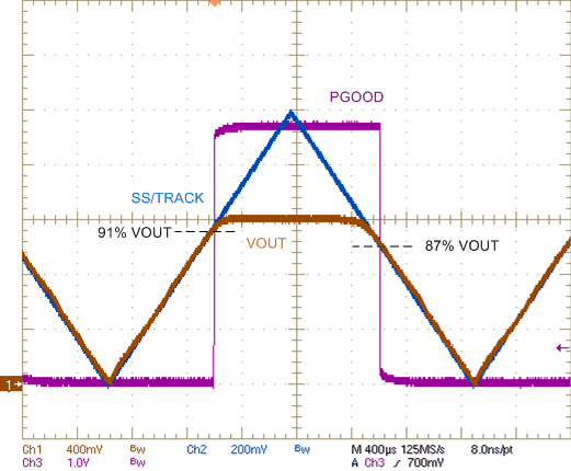 Figure 33. Typical Output Voltage Tracking Waveforms and PGOOD Flag
Two practical tracking configurations, ratiometric and coincident, are shown in Figure 34. The most common application is coincident tracking, used in core vs. I/O voltage tracking in DSP and FPGA implementations. Coincident tracking forces the master and slave channels to have the same output voltage ramp rate until the slave output reaches its regulated setpoint. Conversely, ratiometric tracking sets the slave's output voltage to a fraction of the master's output voltage during startup.
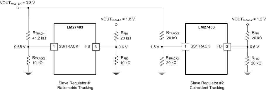 Figure 34. Tracking Implementation With Master, Ratiometric Slave and Coincident Slave Rails
For coincident tracking, connect the slave regulator's SS/TRACK input to a resistor divider from the master's output voltage that is the same as the divider used on the slave's FB pin. In other words, simply select RTRACK1 = RFB1 and RTRACK2 = RFB2 as shown in Figure 34. As the master voltage rises, the slave voltage rises identically. Eventually, the slave voltage reaches its regulation voltage, at which point the internal reference takes over the regulation while the SS/TRACK input continues to increase, thus removing itself from changing the output voltage.
In all cases, to ensure that the output voltage accuracy is not compromised by the SS/TRACK voltage being too close to the 0.6-V reference voltage, the final value of the slave's SS/TRACK voltage should be at least 20 mV above FB.
8.3.12 Monotonic Startup
The LM27403 has monotonic startup capability with no dips or flat spots in the output voltage waveform during startup (including prebiased startup) and fault recovery. During the soft-start interval, FB follows SS/TRACK, and the output voltage linearly increases to the nominal output setpoint. Figure 35 illustrates the output voltage behavior during a monotonic startup to a nominal level of 1.2V. The UVLO/EN pin is driven high by a TTL logic signal. As mentioned previously, the startup time is determined by the use of an external soft-start capacitor at the SS/TRACK pin charged by an internally generated 3-µA constant current source. If a soft-start capacitor is not used, the device automatically enables the internal 7-bit (128 step) digital soft-start. The PGOOD flag transitions high when FB reaches its 91% threshold. As described previously, there is a calibration interval based on four cycles on the D+ pin (that is, 512 clock cycles) that creates a delay from UVLO/EN crossing its precision threshold to SS/TRACK being released.
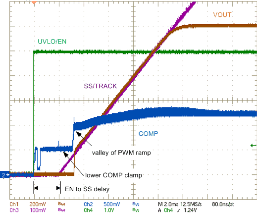 Figure 35. Typical Monotonic Output Voltage Startup Waveforms, 1.2-V Output
8.3.13 Prebias Startup
In certain applications, the output voltage may have an initial voltage prebias before the LM27403 is powered on or enabled. The LM27403 is able to startup into a prebiased load while maintaining a monotonic output voltage startup characteristic.
The LM27403 does not allow switching until the SS/TRACK pin voltage has reached the feedback (FB) voltage level. Once this level is reached, the controller begins to regulate and switch synchronously, allowing a certain amount of negative current during PWM switching operation. Thereafter, the feedback voltage follows the soft-start voltage up to 0.6 V. This is illustrated in Figure 36 where nominal output voltage is 1.2 V and the output voltage waveform represents twice the FB level. The output is not pulled low during a prebiased startup condition. Note that if the output is prebiased to a higher voltage than the nominal level (as set by the feedback resistor divider), the LM27403 does not pull the output low, hence eliminating current flow through parasitic paths in the system.
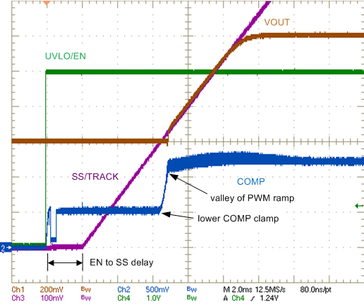 Figure 36. Typical Startup Waveforms With 0.6-V Prebiased Output, 1.2-V Nominal Output
The LM27403 automatically pulls down the SS/TRACK pin to GND before the onset of switching and during a restart from a fault condition. When SS/TRACK is initially released, subsequent to the temperature sense calibration delay, the COMP voltage is released to the lower COMP clamp level and no switching occurs. Both the LG and HG pins are held low while the SS/TRACK voltage stays below the FB voltage level. This action ensures that a prebiased load is not pulled down by a negative dc output current component. When the SS/TRACK pin voltage crosses above either FB or VREF, the COMP voltage slews up to the valley of the PWM ramp and switching begins.
8.3.14 Voltage-Mode Control
The LM27403 incorporates a voltage-mode control loop implementation with input voltage feedforward to eliminate the input voltage dependence of the PWM modulator gain. This configuration allows the controller to maintain stability throughout the entire input voltage operating range and provides for optimal response to input voltage transient disturbances. The constant gain provided by the controller greatly simplifies feedback loop design because loop characteristics remain constant as the input voltage changes, unlike a buck converter without voltage feedforward. An increase in input voltage is matched by a concomitant increase in ramp voltage amplitude to maintain constant modulator gain. The input voltage feedforward gain, kFF, is 1/9, equivalent to the ramp amplitude divided by the input voltage, VRAMP/VIN. See the Control Loop Compensation section for more detail.
8.3.15 Output Voltage Remote Sense: RS
High-current switching power supplies typically use output voltage remote sensing to achieve the greatest accuracy at the point of load. There are usually some finite bus structure resistances between the power supply and load, denoted by lumped elements RBUS+ and RBUS– in Figure 37, that cause unwanted voltage drops or load regulation errors, particularly at high output currents.
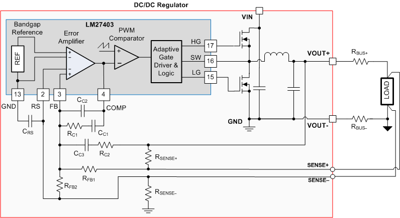 Figure 37. LM27403 Output Remote Sense and Voltage Control Loop
Remote ground sensing is implemented in the LM27403 by bringing another amplifier input, designated RS, outside of the device package to act as a kelvin ground sense. This circuit is created by replacing the standard error amplifier used in the PWM loop with a new amplifier that has two pairs of differential inputs. One of the differential input pairs is used to sense the internal reference voltage relative to the IC ground potential. The other differential input is used to remotely sense the feedback (FB) voltage relative to RS connected to the negative load terminal (at the output point of load). The output of the new error amplifier is the difference between the two pairs of inputs multiplied by some gain factor, and in all other respects works the same as the classic op-amp type error amplifier.
For accurate remote sensing of the output at the load, make sure to tie upper feedback resistor RFB1 directly to the load at the point where output regulation is required. However, in order to minimize injected noise into the high-impedance FB node, connect the RC lead network, RC2 and CC3, typically found across RFB1 in voltage-mode control loop compensation networks, to the local VOUT connection, as shown in Figure 37. Similarly, connect the negative sense line locally at the negative load terminal and route both sense lines as a differential pair to minimize pickup and injected noise. Sense resistors, RSENSE+ and RSENSE–, typically 10 Ω each, are used to maintain regulation when the remote sense lines are not connected or as a fail-safe measure if the lines become disconnected. In particularly noisy environments, capacitor CRS shown in Figure 37 (typically 0.1 µF) is supplemented by a series resistor (for example, 10 Ω). If remote sense is not required, RS is simply shorted to GND.
The configuration in Figure 37 avoids the use of a separate unity-gain differential amplifier, a solution commonly used to perform remote sensing. The offset and gain error of this differential amplifier configuration compound any inaccuracy associated with the reference and error amplifier input offset voltage. The accuracy of the feedback system is not compromised when using the method shown in Figure 37. The LM27403 specified feedback accuracy of ±1% is preserved over the full operating temperature range.
8.3.16 Power Good: PGOOD
To implement an open-drain power-good function for sequencing and fault detection, use the PGOOD pin of the LM27403. The PGOOD open-drain MOSFET is pulled low during current limit, UVLO, output undervoltage and overvoltage, or if the output is not regulated.
More specifically, this function can be triggered by multiple events, including the output voltage either exceeding the overvoltage threshold (117% VREF) or decreasing below the undervoltage threshold (91% VREF), heavy overcurrent, soft-start voltage (both internal and external) below 91% VREF, UVLO, thermal shutdown, enable delay, or disabled state.
To prevent momentary glitches to the PGOOD pin, a 20-µs deglitch filter is built into the LM27403 to prevent multiple triggerings of the flag. Note that the primary objective of PGOOD is to signal to the system that the soft-start period has expired and the output voltage is in regulation for loads within the rated limit. This can be used for sequencing downstream regulators, an example of which is shown schematically in Figure 48.
During soft-start operation, the PGOOD flag is effectively a logic AND of two signals:
- The internal soft-start counter (signals the internal soft-start-done flag when the count reaches 128).
- The UVT comparator output. Note that the UVT comparator monitors SS/TRACK voltage until the first PWM pulse, and then monitors the FB voltage.
The reason for multiplexing the UVT comparator is to support prebias loads and tracking. The PGOOD voltage waveform is shown in Figure 33 with a 100-kΩ pullup resistor to VDD. As described previously, VDD disappears when UVLO/EN is pulled lower than an effective diode drop (~0.7 V). This does not represent a system-level issue because PGOOD is already pulled low in that scenario.
8.3.17 Gate Drivers: LG and HG
The LM27403 gate driver impedances are low enough to perform effectively in high output current applications where large die-size or paralleled MOSFETs with correspondingly large gate charge, QG, are used. Measured at VVDD = 4.5 V, the LM27403's low-side driver has a low impedance pull-down path of 0.9 Ω to minimize the effect of dv/dt induced turn-on, particularly with low gate-threshold voltage MOSFETs. Similarly, the high-side driver has 1.5-Ω and 1.0-Ω pull-up and pull-down impedances, respectively, for faster switching transition times, lower switching loss, and greater efficiency.
Furthermore, there is a proprietary adaptive deadtime control on both switching edges to prevent shoot-through and cross-conduction, minimize body diode conduction time, and reduce body diode reverse recovery related losses. The LM27403 is fully compatible with discrete and Power Block NexFET™ MOSFETs from TI.
8.3.18 Sink and Source Capability
Even though an LM27403-based DC/DC regulator is capable of sinking and sourcing current (as it operates in CCM), the inductor DCR-based overcurrent protection operates only with positive currents. Negative currents are detected through the low-side MOSFET only when the device is in an overvoltage condition (refer to Zero Cross and Negative Current Limit sections). Note that prebias startup still operates normally (refer to Prebias Startup section).
8.4 Device Functional Modes
8.4.1 Fault Conditions
Overcurrent, overtemperature, output undervoltage and overvoltage protection features are included in the LM27403.
8.4.1.1 Thermal Shutdown
The LM27403 includes an internal junction temperature monitor. If the temperature exceeds 150°C (typ), thermal shutdown occurs. When entering thermal shutdown, the device:
- turns off the low-side and high-side MOSFETs;
- flushes the external soft-start capacitor;
- initiates a soft-start sequence when the die temperature decreases by the OTP hysteresis, 20°C (typ).
This is a nonlatching protection, and, as such, the device will cycle into and out of thermal shutdown if the fault persists.
8.4.1.2 Current Limit and Short Circuit Operation (Positive Overcurrent)
When detecting a current-limit (CL) event, one of the following actions occur:
- Light CL: When a current limit event is detected, the high-side on-pulse is immediately terminated (HG off, LG on) and the system continues regulating on the next system clock event;
- Heavy CL: If five current limit events occur in any 32 clock cycles, the pulse is terminated (HG off, LG off) and hiccup mode is entered.
The following actions occur in hiccup mode:
- HG off, LG off;
- Re-enable soft-start clock to count 5-ms timeout for hiccup delay;
- At the end of the hiccup delay, re-enter the startup sequence, including the internal enable delay.
Every time a current limit event is detected, the current limit event counter is incremented on the next clock edge. If the current limit event counter reaches its threshold of five, then the hiccup mode is entered.
8.4.1.3 Negative Current Limit
Negative current limit detection is in effect only after an overvoltage (OV) condition is met. The OV flag is deglitched by 10 µs. By the time OV is signaled, the loop has most likely moved into a low- or zero-percent duty cycle that poses the threat of excessive negative current. Thus, the negative current limit is in effect as soon as the OV condition is detected rather than waiting for the deglitched version. If the negative current limit is exceeded, the low-side MOSFET gate (LG pin) is pulled low and the LM27403 enters Negative Current Limit hiccup mode for 5 ms.
Negative Current Limit hiccup mode (subsequent to OVP) is different from Current Limit hiccup mode in that zero-cross current detection is active in the latter and the LG output is high. However, as with Current Limit hiccup mode, the system attempts to restart after the 5-ms timeout, as described in the Current Limit Handling section. The LM27403 detects a negative current limit by monitoring the switch-node (SW) voltage while the low-side MOSFET is on. If the switch-node voltage (that is, the low-side MOSFET drain-source voltage) rises 100 mV above ground during the low-side MOSFET conduction interval, the comparator trips, signaling that the negative current limit threshold has been reached. The low-side MOSFET is turned off, thus protecting it from excess current.
The negative current comparator is valid only when the LG is high. Blanking time lasts 20 ns to 50 ns after LG has been asserted. Blanking recurs as soon as PWM goes high.
8.4.1.4 Undervoltage Threshold (UVT)
The FB pin is also monitored for an output voltage excursion below the nominal level. However, if the UVT comparator is tripped, no action occurs on the normal switching cycles. The UVT signal is used solely as a valid condition for the Power Good flag to transition low. When the FB voltage exceeds 91% of the reference voltage, the Power Good flag transitions high. Conversely, the Power Good flag transitions low when the FB voltage is less than 87% of the reference.
8.4.1.5 Overvoltage Threshold (OVT)
When the FB voltage exceeds 116.5% of the reference voltage, the Power Good flag transitions low after a 10-µs deglitch. The control loop attempts to bring the output voltage back to the nominal setpoint. Conversely, when the FB voltage goes below 113% of the reference, the Power Good flag is allowed to transition high. Negative current-limit detection is activated when the regulator is in an OV condition. See the Negative Current Limit section for more details.