JAJSBC2L March 2000 – January 2018 LM317L-N
PRODUCTION DATA.
- 1 特長
- 2 アプリケーション
- 3 概要
- 4 改訂履歴
- 5 Pin Configuration and Functions
- 6 Specifications
- 7 Detailed Description
-
8 Application and Implementation
- 8.1 Application Information
- 8.2
Typical Applications
- 8.2.1 1.25-V to 25-V Adjustable Regulator
- 8.2.2 Digitally-Selected Outputs
- 8.2.3 High Gain Amplifier
- 8.2.4 Adjustable Current Limiter
- 8.2.5 Precision Current Limiter
- 8.2.6 Slow Turnon 15-V Regulator
- 8.2.7 Adjustable Regulator With Improved Ripple Rejection
- 8.2.8 High Stability 10-V Regulator
- 8.2.9 Adjustable Regulator With Current Limiter
- 8.2.10 0-V to 30-V Regulator
- 8.2.11 Regulator With 15-mA Short-Circuit Current
- 8.2.12 Power Follower
- 8.2.13 Adjusting Multiple On-Card Regulators With Single Control
- 8.2.14 100-mA Current Regulator
- 8.2.15 1.2-V to 12-V Regulator With Minimum Program Current
- 8.2.16 50-mA Constant Current Battery Charger for Nickel-Cadmium Batteries
- 8.2.17 5-V Logic Regulator With Electronic Shutdown
- 8.2.18 Current-Limited 6-V Charger
- 8.2.19 Short Circuit-Protected 80-V Supply
- 8.2.20 Basic High-Voltage Regulator
- 8.2.21 Precision High-Voltage Regulator
- 8.2.22 Tracking Regulator
- 8.2.23 Regulator With Trimmable Output Voltage
- 8.2.24 Precision Reference With Short-Circuit Proof Output
- 8.2.25 Fully-Protected (Bulletproof) Lamp Driver
- 8.2.26 Lamp Flasher
- 9 Power Supply Recommendations
- 10Layout
- 11デバイスおよびドキュメントのサポート
- 12メカニカル、パッケージ、および注文情報
パッケージ・オプション
メカニカル・データ(パッケージ|ピン)
サーマルパッド・メカニカル・データ
発注情報
7.1 Overview
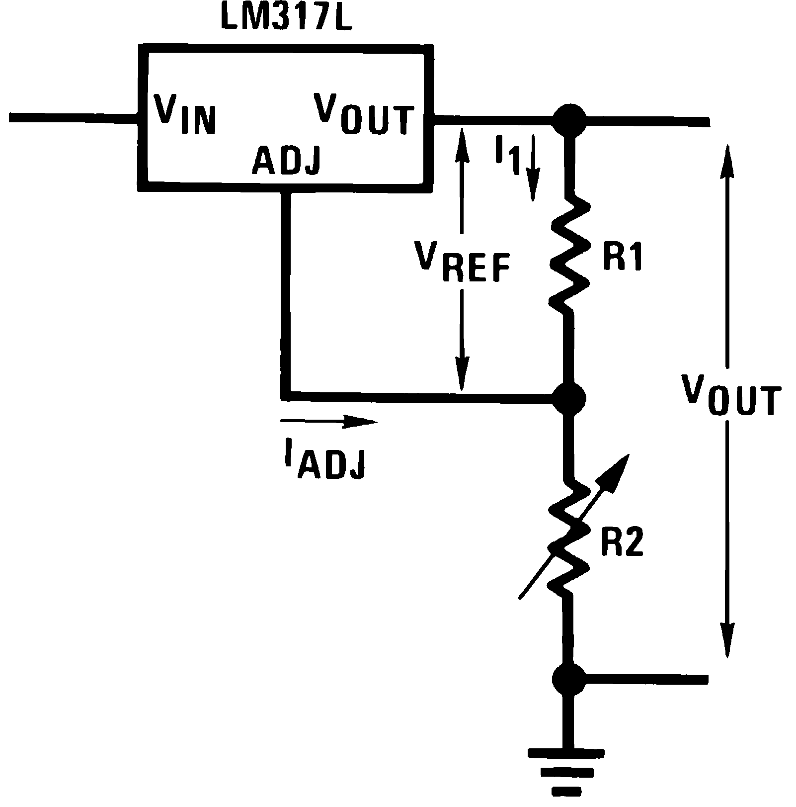
In operation, the LM317L-N develops a nominal 1.25-V reference voltage, VREF, between the output and adjustment terminal. The reference voltage is impressed across program resistor R1 and, because the voltage is constant, a constant current I1 then flows through the output set resistor R2, giving an output voltage of:

Because the 100-μA current from the adjustment terminal represents an error term, the LM317L-N was designed to minimize IADJ and make it very constant with line and load changes. To do this, all quiescent operating current is returned to the output establishing a minimum load current requirement. If there is insufficient load on the output, the output will rise.
 Figure 13. Typical Application Circuit for Adjustable Regulator