SNOSBJ2B August 2000 – January 2016 LM119
PRODUCTION DATA.
- 1Features
- 2Description
- 3Revision History
- 4Pin Configuration and Functions
- 5Specifications
- 6Detailed Description
- 7Application and Implementation
- 8Device and Documentation Support
- 9Mechanical, Packaging, and Orderable Information
パッケージ・オプション
メカニカル・データ(パッケージ|ピン)
サーマルパッド・メカニカル・データ
発注情報
5 Specifications
5.1 Absolute Maximum Ratings
over operating free-air temperature range (unless otherwise noted)(1)(2)(3)| MIN | MAX | UNIT | ||
|---|---|---|---|---|
| Total supply voltage | 36 | V | ||
| Output to negative supply voltage | 36 | V | ||
| Ground to negative supply voltage | 25 | V | ||
| Ground to positive supply voltage | 18 | V | ||
| Differential input voltage | –5 | +5 | V | |
| Input voltage(4) | –15 | +15 | V | |
| Power dissipation(5) | 500 | mW | ||
| Output short circuit duration | 10 | sec | ||
| Lead temperature (soldering, 10 sec.) | 260 | °C | ||
| Soldering information(6) | Dual-In-Line Package Soldering (10 seconds) | 260 | °C | |
| Small Outline Package Vapor Phase (60 seconds) | 215 | |||
| Small Outline Package Infrared (15 seconds) | 220 | |||
| Operating temperature | LM119 | –55 | 125 | °C |
| LM219 | –25 | 85 | ||
| LM319A, LM319 | 0 | 70 | ||
| Storage temperature, Tstg | –65 | 150 | °C | |
(1) Stresses beyond those listed under Absolute Maximum Ratings may cause permanent damage to the device. These are stress ratings only, which do not imply functional operation of the device at these or any other conditions beyond those indicated under Recommended Operating Conditions. Exposure to absolute-maximum-rated conditions for extended periods may affect device reliability.
(2) If Military/Aerospace specified devices are required, please contact the Texas Instruments Sales Office/ Distributors for availability and specifications.
(3) Refer to RETS119X for LM119H/883 and LM119J/883 specifications.
(4) For supply voltages less than ±15 V the absolute maximum input voltage is equal to the supply voltage.
(5) The maximum junction temperature of the LM119 is 150°C, while that of the LM219 is 110°C. For operating at elevated temperatures, devices in the H10 package must be derated based on a thermal resistance of 160°C/W, junction to ambient, or 19°C/W, junction to case. The thermal resistance of the J14 and N14 packages is 100°C/W, junction to ambient.
(6) See AN-450 “Surface Mounting Methods and Their Effect on Product Reliability” for other methods of soldering surface mount devices.
5.2 ESD Ratings
| VALUE | UNIT | |||
|---|---|---|---|---|
| V(ESD) | Electrostatic discharge | Human body model (HBM), per ANSI/ESDA/JEDEC JS-001(1) | ±800 | V |
(1) JEDEC document JEP155 states that 500-V HBM allows safe manufacturing with a standard ESD control process.
5.3 Thermal Information
| THERMAL METRIC(1) | LM119, LM219, LM319 | UNIT | |||
|---|---|---|---|---|---|
| TO-100 (LME) |
PDIP (NFF) |
CDIP (J) |
|||
| 10 PINS | 14 PINS | 14 PINS | |||
| RθJA | Junction-to-ambient thermal resistance | 160 | 100 | 100 | °C/W |
| RθJC(top) | Junction-to-case (top) thermal resistance | 19 | NA | NA | °C/W |
(1) For more information about traditional and new thermal metrics, see the Semiconductor and IC Package Thermal Metrics application report, SPRA953.
5.4 Electrical Characteristics LM119, LM219
These specifications apply for VS = ±15 V, and the Ground pin at ground, and −55°C ≤ TA ≤ +125°C, unless otherwise stated. With the LM219, all temperature specifications are limited to −25°C ≤ TA ≤ +85°C. The offset voltage, offset current and bias current specifications apply for any supply voltage from a single 5-V supply up to ±15-V supplies. Do not operate the device with more than 16 V from ground to VS.| PARAMETER | TEST CONDITIONS | MIN | TYP | MAX | UNIT | |
|---|---|---|---|---|---|---|
| Input Offset Voltage(1) | TA = 25°C, RS ≤ 5k | 0.7 | 4 | mV | ||
| Input Offset Current(1) | TA = 25°C | 30 | 75 | nA | ||
| Input Bias Current | TA = 25°C | 150 | 500 | nA | ||
| Voltage Gain | TA = 25°C(2) | 10 | 40 | V/mV | ||
| Response Time(3) | TA = 25°C, VS = ±15 V | 80 | ns | |||
| Saturation Voltage | VIN ≤ −5 mV, IOUT = 25 mA TA = 25°C |
0.75 | 1.5 | V | ||
| Output Leakage Current | VIN ≥ 5 mV, VOUT = 35 V TA = 25°C |
0.2 | 2 | µA | ||
| Input Offset Voltage(1) | RS ≤ 5k | 7 | mV | |||
| Input Offset Current(1) | 100 | nA | ||||
| Input Bias Current | 1000 | nA | ||||
| Input Voltage Range | VS = ±15 V | –12 | ±13 | +12 | V | |
| V+ = 5 V, V- = 0 | 1 | 3 | ||||
| Saturation Voltage | V+ ≥ 4.5 V, V− = 0 VIN ≤ −6 mV, ISINK ≤ 3.2 mA |
V | ||||
| TA ≥ 0°C | 0.23 | 0.4 | ||||
| TA ≤ 0°C | 0.6 | |||||
| Output Leakage Current | VIN ≥ 5 mV, VOUT = 35 V, V− = VGND = 0 V | 1 | 10 | µA | ||
| Differential Input Voltage | ±5 | V | ||||
| Positive Supply Current | TA = 25°C, V+ = 5 V, V− = 0 | 4.3 | mA | |||
| Positive Supply Current | TA = 25°C, VS = ±15 V | 8 | 11.5 | mA | ||
| Negative Supply Current | TA = 25°C, VS = ±15 V | 3 | 4.5 | mA | ||
(1) The offset voltages and offset currents given are the maximum values required to drive the output within a volt of either supply with a 1-mA load. Thus, these parameters define an error band and take into account the worst case effects of voltage gain and input impedance.
(2) Output is pulled up to 15 V through a 1.4-kW resistor.
(3) The response time specified is for a 100-mV input step with 5-mV overdrive.
5.5 Electrical Characteristics LM319, LM319A
These specifications apply for VS = ±15 V, and 0°C ≤ TA ≤ 70°C, unless otherwise stated. The offset voltage, offset current, and bias current specifications apply for any supply voltage from a single 5-V supply up to ±15-V supplies. Do not operate the device with more than 16 V from ground to VS.| PARAMETER | TEST CONDITIONS | LM319A | LM319 | UNIT | |||||
|---|---|---|---|---|---|---|---|---|---|
| MIN | TYP | MAX | MIN | TYP | MAX | ||||
| Input Offset Voltage(1) | TA = 25°C, RS ≤ 5k | 0.5 | 1 | 2 | 8 | mV | |||
| Input Offset Current(1) | TA = 25°C | 20 | 40 | 80 | 200 | nA | |||
| Input Bias Current | TA = 25°C | 150 | 500 | 250 | 1000 | nA | |||
| Voltage Gain | TA = 25°C(2) | 20 | 40 | 8 | 40 | V/mV | |||
| Response Time(3) | TA = 25°C, VS = ±15 V | 80 | 80 | ns | |||||
| Saturation Voltage | VIN ≤ −10 mV, IOUT = 25 mA TA = 25°C |
0.75 | 1.5 | 0.75 | 1.5 | V | |||
| Output Leakage Current | VIN ≥ 10 mV, VOUT = 35 V V− = VGND = 0 V, TA = 25°C |
0.2 | 10 | 0.2 | 10 | µA | |||
| Input Offset Voltage(1) | RS ≤ 5k | 10 | 10 | mV | |||||
| Input Offset Current(1) | 300 | 300 | nA | ||||||
| Input Bias Current | 1000 | 1200 | nA | ||||||
| Input Voltage Range | VS = ±15 V | ±13 | ±13 | V | |||||
| V+ = 5 V, V- = 0 | 1 | 3 | 1 | 3 | |||||
| Saturation Voltage | V+ ≥ 4.5 V, V− = 0 VIN ≤ −10 mV, ISINK ≤ 3.2 mA |
0.3 | 0.4 | 0.3 | 0.4 | V | |||
| Differential Input Voltage | ±5 | ±5 | V | ||||||
| Positive Supply Current | TA = 25°C, V+ = 5 V, V− = 0 | 4.3 | 4.3 | mA | |||||
| Positive Supply Current | TA = 25°C, VS = ±15 V | 8 | 12.5 | 8 | 12.5 | mA | |||
| Negative Supply Current | TA = 25°C, VS = ±15 V | 3 | 5 | 3 | 5 | mA | |||
5.6 Typical Characteristics
Typical Characteristics – LM119, LM119A, LM219
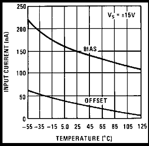 Figure 1. Input Currents
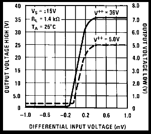 Figure 3. Transfer Function
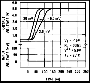 Figure 5. Response Time for Various Input Overdrives
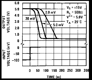 Figure 7. Response Time for Various Input Overdrives
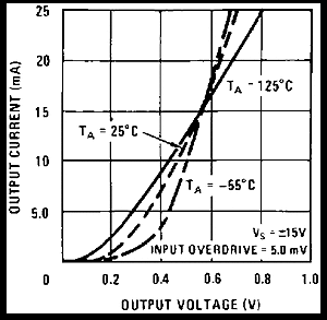 Figure 9. Output Saturation Voltage
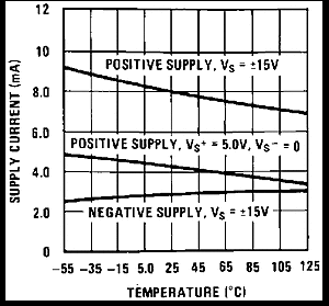 Figure 11. Supply Current
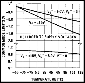 Figure 2. Common-Mode Limits
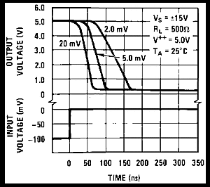 Figure 4. Response Time for Various Input Overdrives
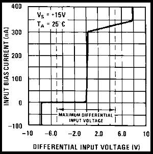 Figure 6. Input Characteristics
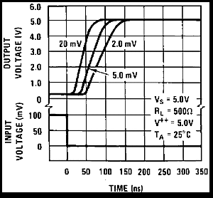 Figure 8. Response Time for Various Input Overdrives
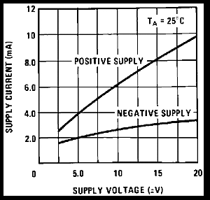 Figure 10. Supply Current
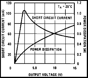 Figure 12. Output Limiting Characteristics
5.6.1 Typical Characteristics – LM319, LM319A
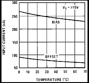 Figure 13. Input Currents
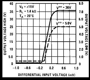 Figure 15. Transfer Function
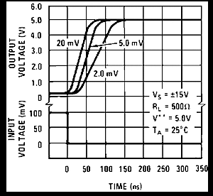 Figure 17. Response Time for Various Input Overdrives
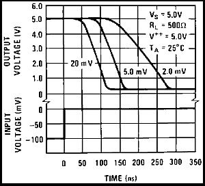 Figure 19. Response Time for Various Input Overdrives
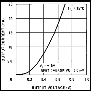 Figure 21. Output Saturation Voltage
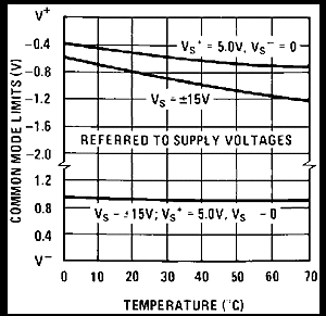 Figure 23. Common-Mode Limits
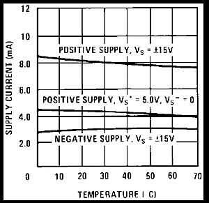 Figure 14. Supply Currents
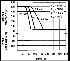 Figure 16. Response Time for Various Input Overdrives
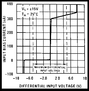 Figure 18. Input Characteristics
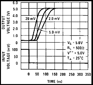 Figure 20. Response Time for Various Input Overdrives
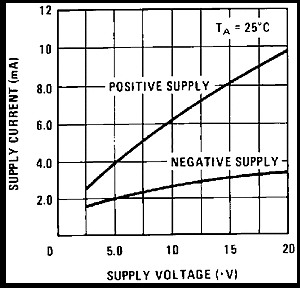 Figure 22. Supply Current
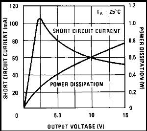 Figure 24. Output Limiting Characteristics