SNOSB38C January 2009 – November 2017 LM3241
PRODUCTION DATA.
- 1 Features
- 2 Applications
- 3 Description
- 4 Revision History
- 5 Pin Configuration and Functions
- 6 Specifications
- 7 Detailed Description
- 8 Application and Implementation
- 9 Power Supply Recommendations
- 10Layout
- 11Device and Documentation Support
- 12Mechanical, Packaging, and Orderable Information
6 Specifications
6.1 Absolute Maximum Ratings
See (1) and (2).| MIN | MAX | UNIT | ||
|---|---|---|---|---|
| Pin voltage | VIN to GND | –0.2 | 6 | V |
| EN, FB, VCON, SW | (GND − 0.2) | (VIN + 0.2)(3) | ||
| Continuous power dissipation(4) | Internally limited | |||
| Junction temperature, TJ-MAX | 150 | °C | ||
| Storage temperature, Tstg | –65 | 150 | °C | |
(1) Stresses beyond those listed under Absolute Maximum Ratings may cause permanent damage to the device. These are stress ratings only, which do not imply functional operation of the device at these or any other conditions beyond those indicated under Recommended Operating Conditions. Exposure to absolute-maximum-rated conditions for extended periods may affect device reliability.
(2) All voltages are with respect to the potential at the GND pins.
(3) All pins are limited to the 6-V maximum stated for the VIN supply.
(4) Internal thermal shutdown circuitry protects the device from permanent damage. Thermal shutdown engages at TJ = 150°C (typ.) and disengages at TJ = 125°C (typical).
6.2 ESD Ratings
| VALUE | UNIT | |||
|---|---|---|---|---|
| V(ESD) | Electrostatic discharge | Human-body model (HBM), per ANSI/ESDA/JEDEC JS-001(1)(2) | 2000 | V |
| Charged-device model (CDM), per JEDEC specification JESD22-C101(3) | 1250 | |||
(1) JEDEC document JEP155 states that 500-V HBM allows safe manufacturing with a standard ESD control process.
(2) The human body model is a 100-pF capacitor discharged through a 1.5-kΩ resistor into each pin. (MIL-STD-883 3015.7).
(3) JEDEC document JEP157 states that 250-V CDM allows safe manufacturing with a standard ESD control process.
6.3 Recommended Operating Conditions
See (1).| MIN | NOM | MAX | UNIT | ||
|---|---|---|---|---|---|
| Input voltage | 2.7 | 5.5 | V | ||
| Recommended load current | 0 | 750 | mA | ||
| TJ | Junction temperature | –40 | 125 | °C | |
| TA | Ambient temperature(2) | –40 | 85 | °C | |
(1) All voltages are with respect to the potential at the GND pins.
(2) In applications where high power dissipation and/or poor package thermal resistance is present, the maximum ambient temperature may have to be de-rated. Maximum ambient temperature (TA-MAX) is dependent on the maximum operating junction temperature (TJ-MAX-OP = 125°C), the maximum power dissipation of the device in the application (PD-MAX), and the junction-to ambient thermal resistance of the part/package in the application (RθJA), as given by the following equation: TA-MAX = TJ-MAX-OP – (RθJA × PD-MAX).
6.4 Thermal Information
| THERMAL METRIC(1) | LM3241 | UNIT | |
|---|---|---|---|
| YZR (DSBGA) | |||
| 6 PINS | |||
| RθJA | Junction-to-ambient thermal resistance | 117 | °C/W |
| RθJC(top) | Junction-to-case (top) thermal resistance | 1 | °C/W |
| RθJB | Junction-to-board thermal resistance | 32.5 | °C/W |
| ψJT | Junction-to-top characterization parameter | 0.2 | °C/W |
| ψJB | Junction-to-board characterization parameter | 32.6 | °C/W |
| RθJC(bot) | Junction-to-case (bottom) thermal resistance | — | °C/W |
(1) For more information about traditional and new thermal metrics, see the Semiconductor and IC Package Thermal Metrics application report.
6.5 Electrical Characteristics
All voltages are with respect to the potential at the GND pins. Minimum (MIN) and maximum (MAX) limits are specified by design, test, or statistical analysis. For performance over the input voltage range and closed-loop results, see the curves in the Typical Characteristics section.| PARAMETER | TEST CONDITIONS | MIN | TYP | MAX | UNIT | |
|---|---|---|---|---|---|---|
| VFB,MIN | Feedback voltage at minimum setting | PWM mode, VCON = 0.24 V | 0.6 | V | ||
| PWM mode, open loop conditions at VIN = 3.6 V, VCON = 0.24 V | 0.58 | 0.62 | ||||
| VFB,MAX | Feedback voltage at maximum setting | PWM mode, VCON = 1.36 V, VIN = 3.9 V | 3.4 | V | ||
| PWM mode, open loop conditions at VIN = 3.6 V, VCON = 1.36 V, VIN = 3.9 V | 3.332 | 3.468 | ||||
| ISHDN | Shutdown supply current | EN = SW = VCON = 0 V(1) | 0.1 | µA | ||
| open loop conditions at VIN = 3.6 V, EN = SW = VCON = 0 V(1) |
2 | |||||
| IQ_PWM | PWM mode quiescent current | PWM mode, No switching(2), VCON = 0 V, FB = 1 V |
620 | µA | ||
| PWM mode, open loop conditions at VIN = 3.6 V, No switching(2), VCON = 0 V, FB = 1 V | 750 | |||||
| IQ_ECO | Eco-mode quiescent current | Eco-mode, No switching(2), VCON = 0.8 V, FB = 2.05 V |
45 | µA | ||
| Eco-mode, open loop conditions at VIN = 3.6 V, No switching(2), VCON = 0.8 V, FB = 2.05 V | 60 | |||||
| RDSON (P) | Pin-pin resistance for PFET | VIN = VGS = 3.6 V, ISW = 200 mA | 160 | mΩ | ||
| Open loop conditions at VIN = 3.6 V, VIN = VGS = 3.6 V, ISW = 200 mA |
250 | |||||
| RDSON (N) | Pin-pin resistance for NFET | VIN = VGS = 3.6 V, ISW = −200 mA | 110 | mΩ | ||
| Open loop conditions at VIN = 3.6 V, VIN = VGS = 3.6 V, ISW = −200 mA |
200 | |||||
| ILIM | PFET switch peak current limit(3) | 1450 | mA | |||
| Open loop conditions at VIN = 3.6 V | 1300 | 1600 | ||||
| FOSC | Internal oscillator frequency | 6 | MHz | |||
| Open loop conditions at VIN = 3.6 V | 5.7 | 6.3 | ||||
| VIH | EN Logic high input threshold | Open loop conditions at VIN = 3.6 V | 1.2 | V | ||
| VIL | EN Logic low input threshold | Open loop conditions at VIN = 3.6 V | 0.4 | V | ||
| Gain | VCON to VOUT gain | 0.24 V ≤ VCON ≤ 1.36 V | 2.5 | V/V | ||
| ICON | VCON pin leakage current | Open-loop mode, VCON = 1 V | ±1 | µA | ||
(1) Shutdown current includes leakage current of PFET.
(2) IQ specified here is when the part is not switching under test mode conditions. For operating quiescent current at no load, see the curves in the Typical Characteristics section.
(3) Current limit is built-in, fixed, and not adjustable.
6.6 System Characteristics
The following spec table entries are specified by design providing the component values in Figure 29 are used. These parameters are not verified by production testing. Minimum (MIN) and maximum (MAX) values apply over the full operating ambient temperature range (–40°C ≤ TA ≤ 85°C) and over the VIN range of 2.7 V to 5.5 V unless otherwise specified. L = 0.47 µH, DCR = 50 mΩ, CIN = 10 µF, 6.3 V, 0603 (1608), COUT = 4.7 µF, 6.3 V, 0603 (1608).| PARAMETER | TEST CONDITIONS | MIN | TYP | MAX | UNIT | |
|---|---|---|---|---|---|---|
| TCON TR | VOUT step rise time from 0.6 V to 3.4 V (to reach 3.26 V) | VIN = 3.6 V, VCON = 0.24 V to 1.36 V, VCON TR = 1 µs, RLOAD = 10 Ω, –30°C ≤ TA ≤ 85°C |
25 | µs | ||
| VIN = 3.6 V, VCON = 0.24 V to 1.36 V, VCON TR = 1 µs, RLOAD = 10 Ω |
30 | |||||
| VOUT step fall time from 3.4 V to 0.6 V (to reach 0.74 V) |
VIN = 3.6 V, VCON = 1.36 V to 0.24 V, VCON TF = 1 µs, RLOAD = 10 Ω, –30°C ≤ TA ≤ 85°C |
25 | ||||
| VIN = 3.6 V, VCON = 1.36 V to 0.24 V, VCON TF = 1 µs, RLOAD = 10 Ω |
30 | |||||
| D | Maximum Duty cycle | 100% | ||||
| IOUT | Maximum output current capability | 2.7 V ≤ VIN ≤ 5.5 V, 0.24 V ≤ VCON ≤ 1.36 V | 750 | mA | ||
| CCON | VCON input capacitance | VCON = 1 V, Test frequency = 100 KHz | 5 | 10 | pF | |
| Linearity | Linearity in control range 0.24 V to 1.36 V | Monotronic in nature(1) | –3% | 3% | ||
| –50 | +50 | mV | ||||
| TON | Turnon time (time for output to reach 95% final value after Enable low-to-high transition) | EN = Low-to-High, VIN = 4.2 V, VOUT = 3.4 V, IOUT = < 1 mA, COUT = 4.7 µF, –30°C ≤ TA ≤ 85°C |
50 | µs | ||
| EN = Low-to-High, VIN = 4.2 V, VOUT = 3.4 V, IOUT = < 1 mA, COUT = 4.7 µF |
55 | |||||
| η | Efficiency | VIN = 3.6 V, VOUT = 0.8 V, IOUT = 10 mA, Eco-mode |
75% | |||
| VIN = 3.6 V, VOUT = 1.8 V, IOUT = 200 mA, PWM mode |
90% | |||||
| VIN = 3.9 V, VOUT = 3.3 V, IOUT = 500 mA, PWM mode |
95% | |||||
| LINE TR | Line transient response | VIN = 3.6 V to 4.2 V, TR = TF = 10 µs, IOUT = 100 mA, VOUT = 0.8 V |
50 | mVpk | ||
| LOAD TR | Load transient response | VIN = 3.1 V/3.6 V/4.5 V, VOUT = 0.8 V, IOUT = 50 mA to 150 mA, TR = TF = 0.1 µs |
50 | |||
(1) Linearity limits are ±3% or ±50 mV whichever is larger.
6.7 Typical Characteristics
VIN = EN = 3.6 V and TA = 25°C, unless otherwise noted.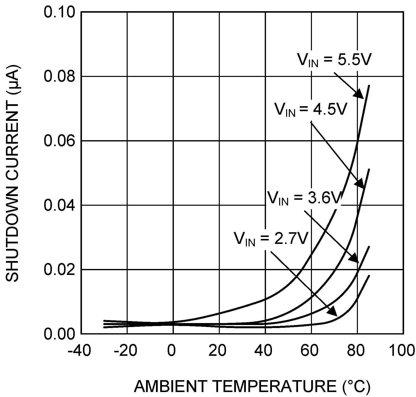
| SW = VCON = EN = 0 V |
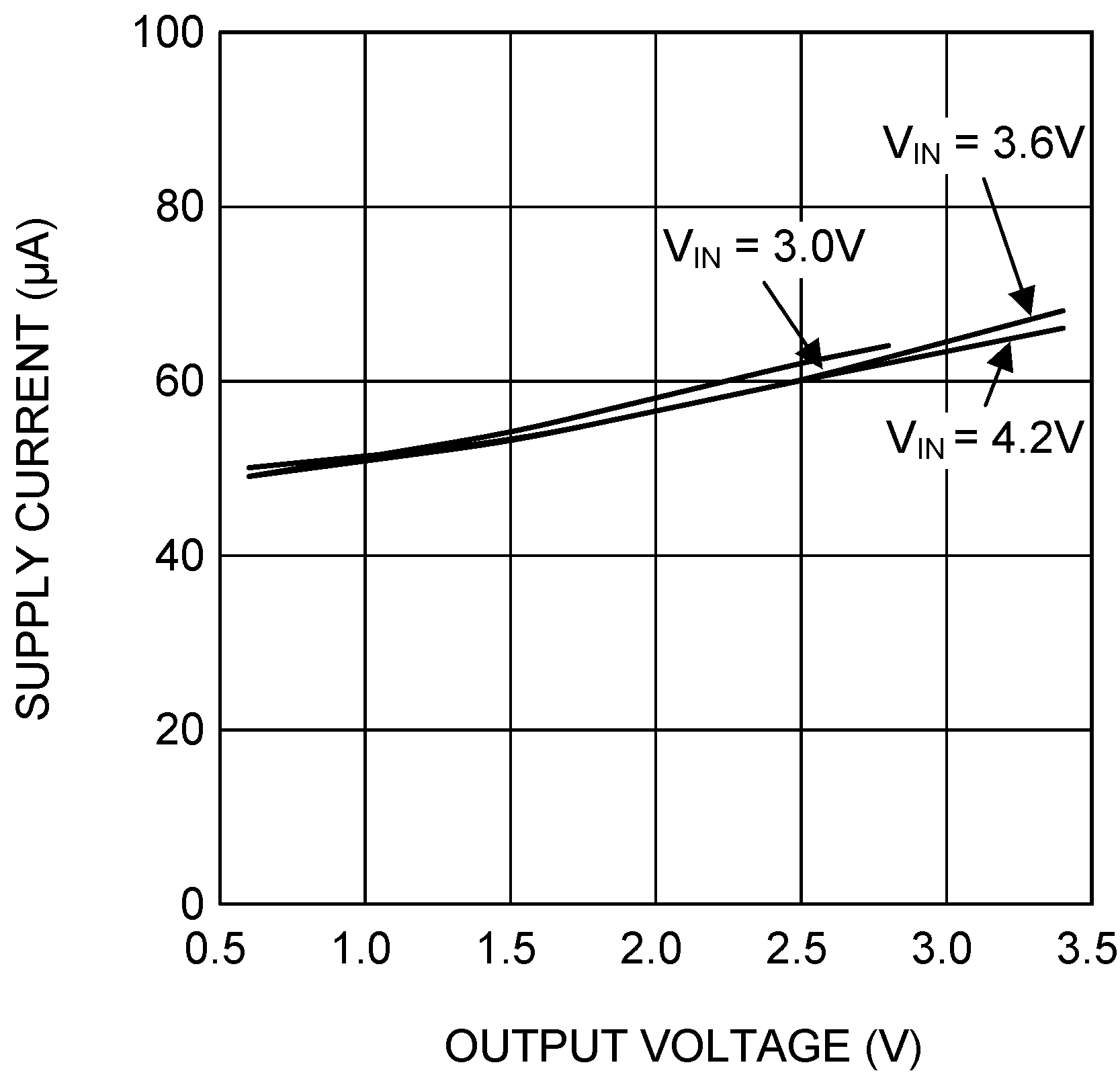
| Closed loop | Switching | No load |
| VOUT = 2 V | RLOAD = 10 Ω |
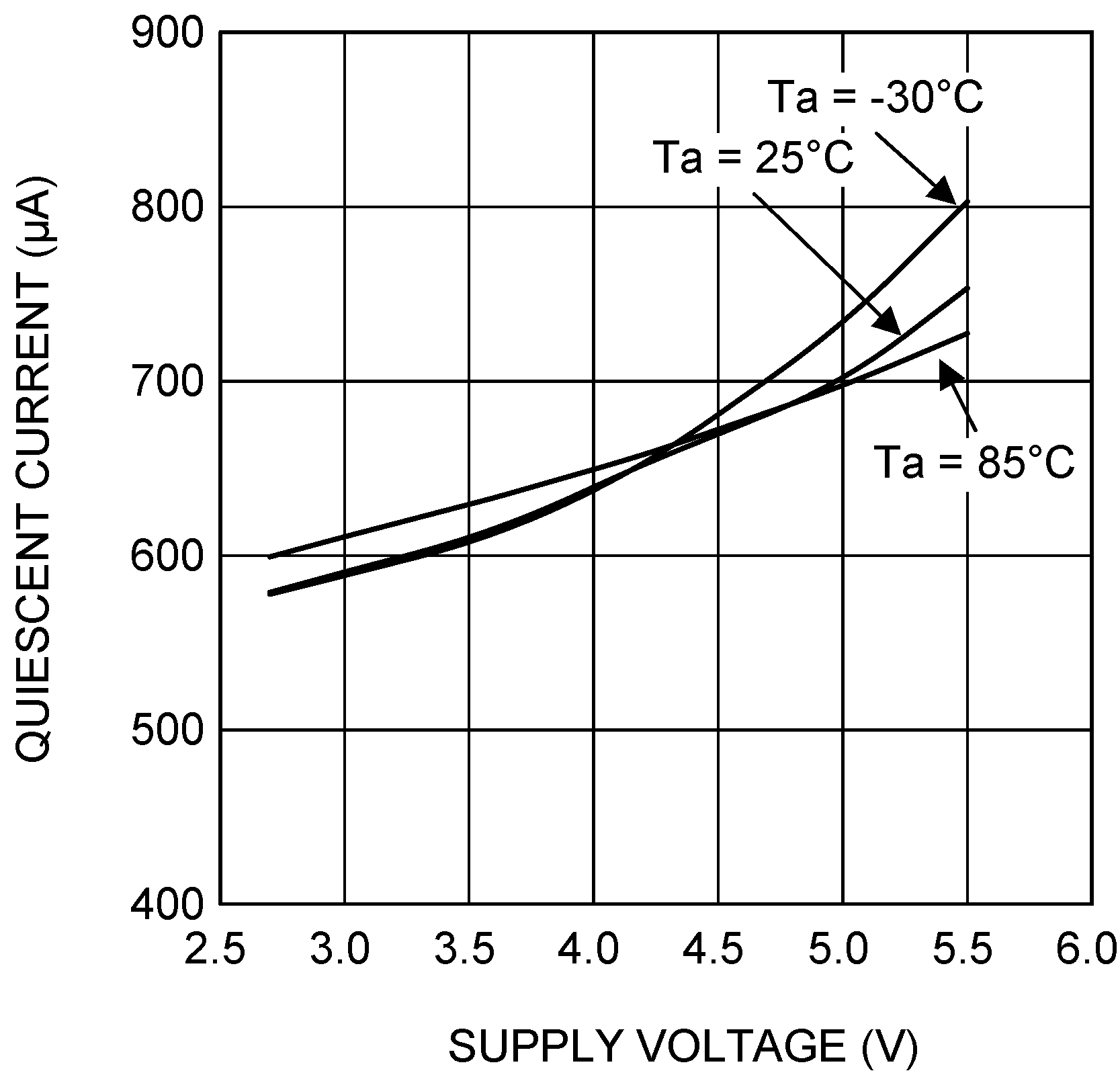
| No switching | FB = 1 V | VCON = 0 V |
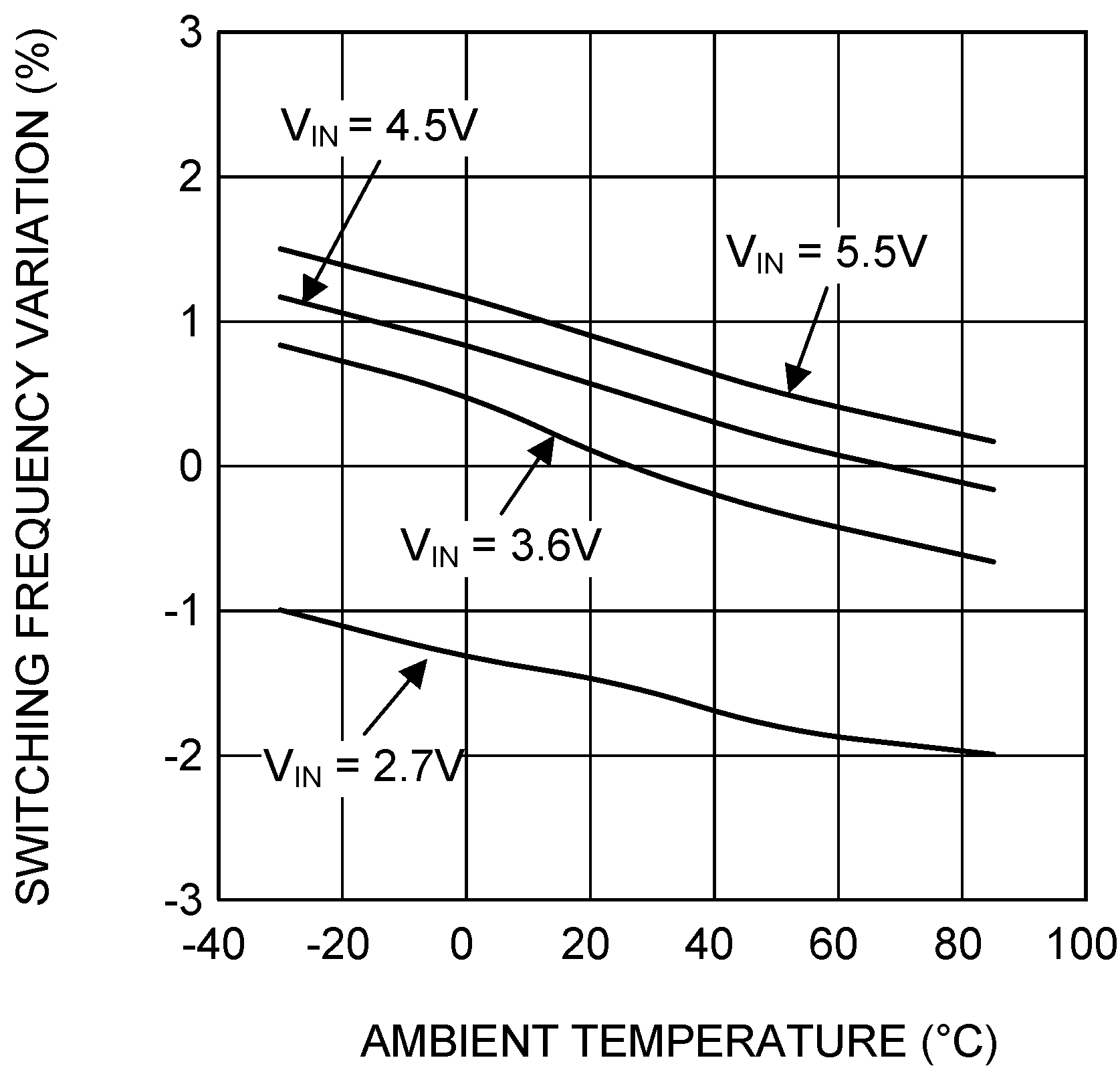
| VOUT = 2 V | IOUT = 200 mA |
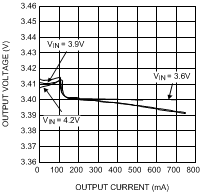
| VOUT = 3.4 V |
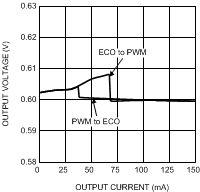
| VOUT = 0.6 V |
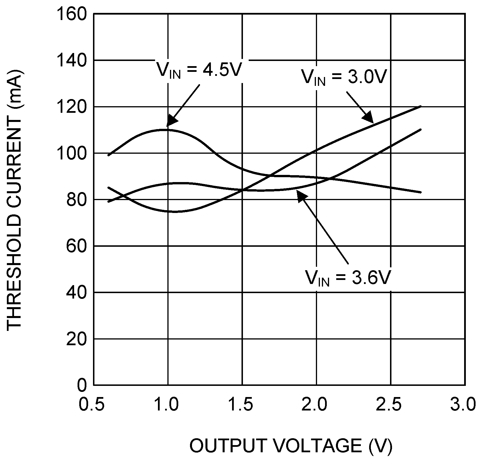
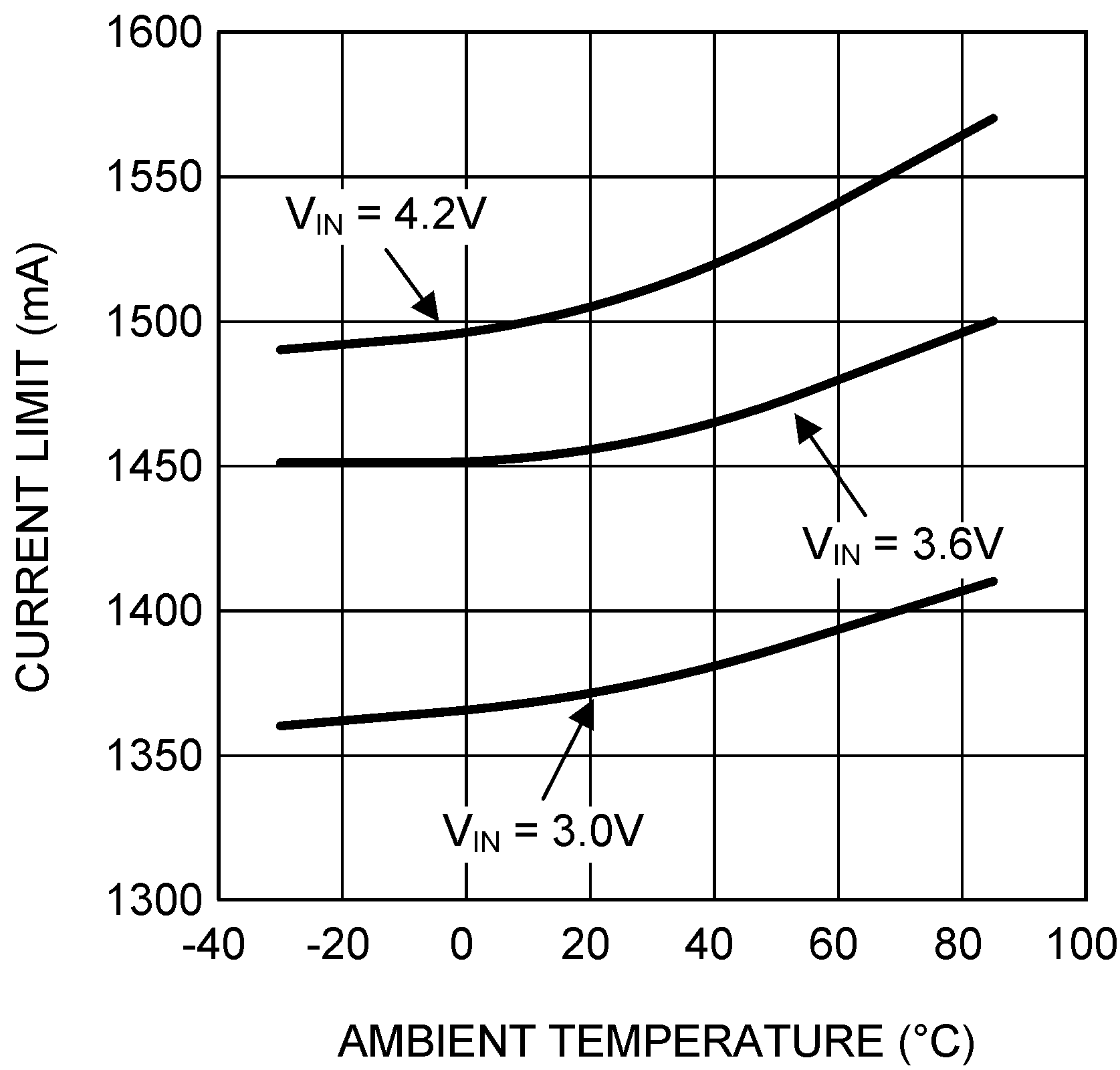
| VOUT = 2 V |
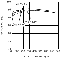
| VOUT = 3.3 V |
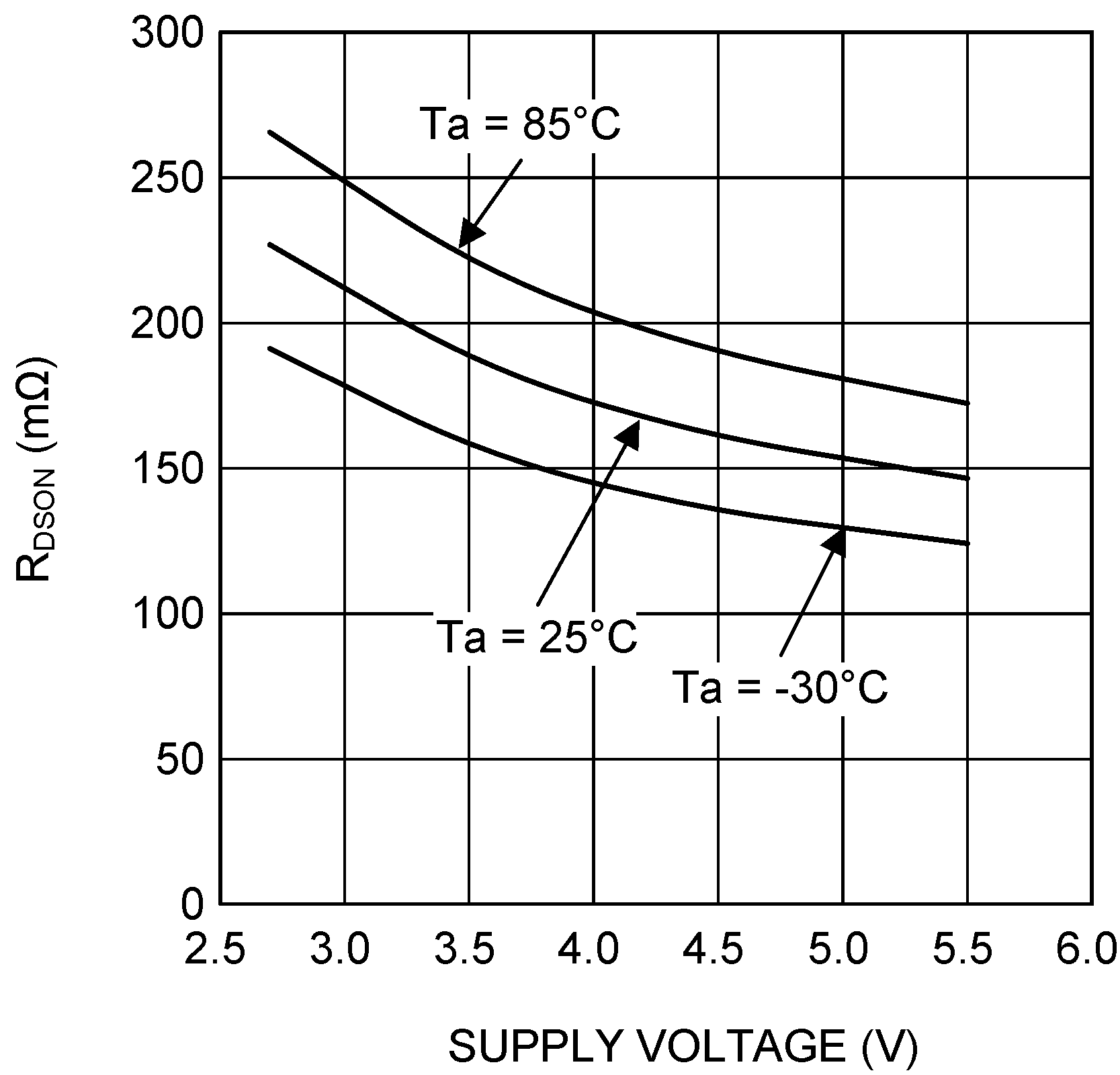
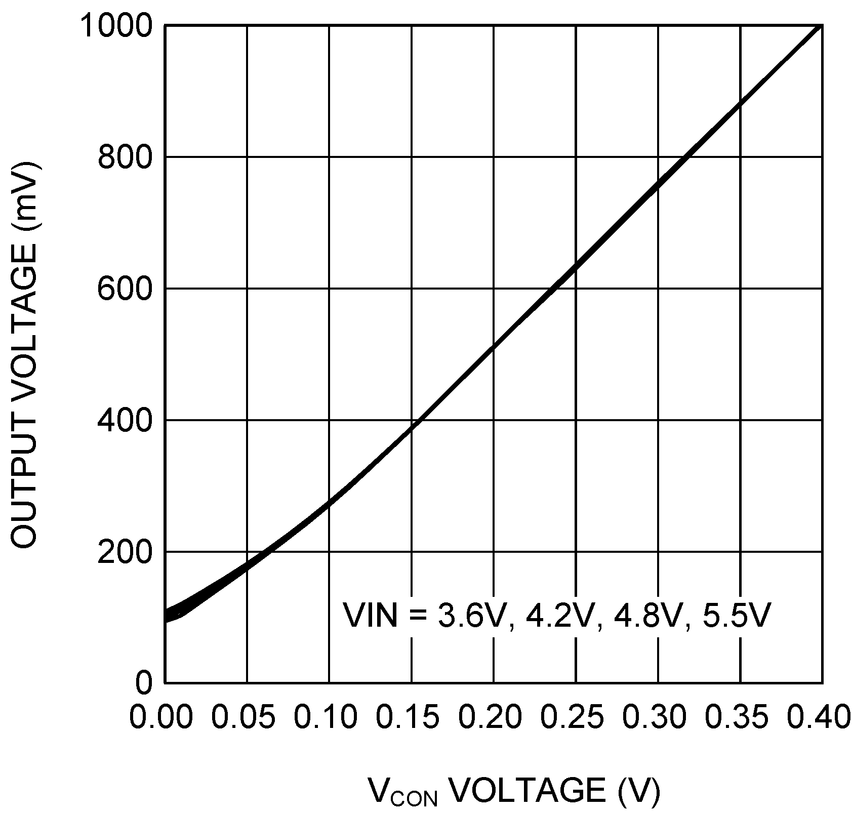
| RLOAD = 10 Ω |
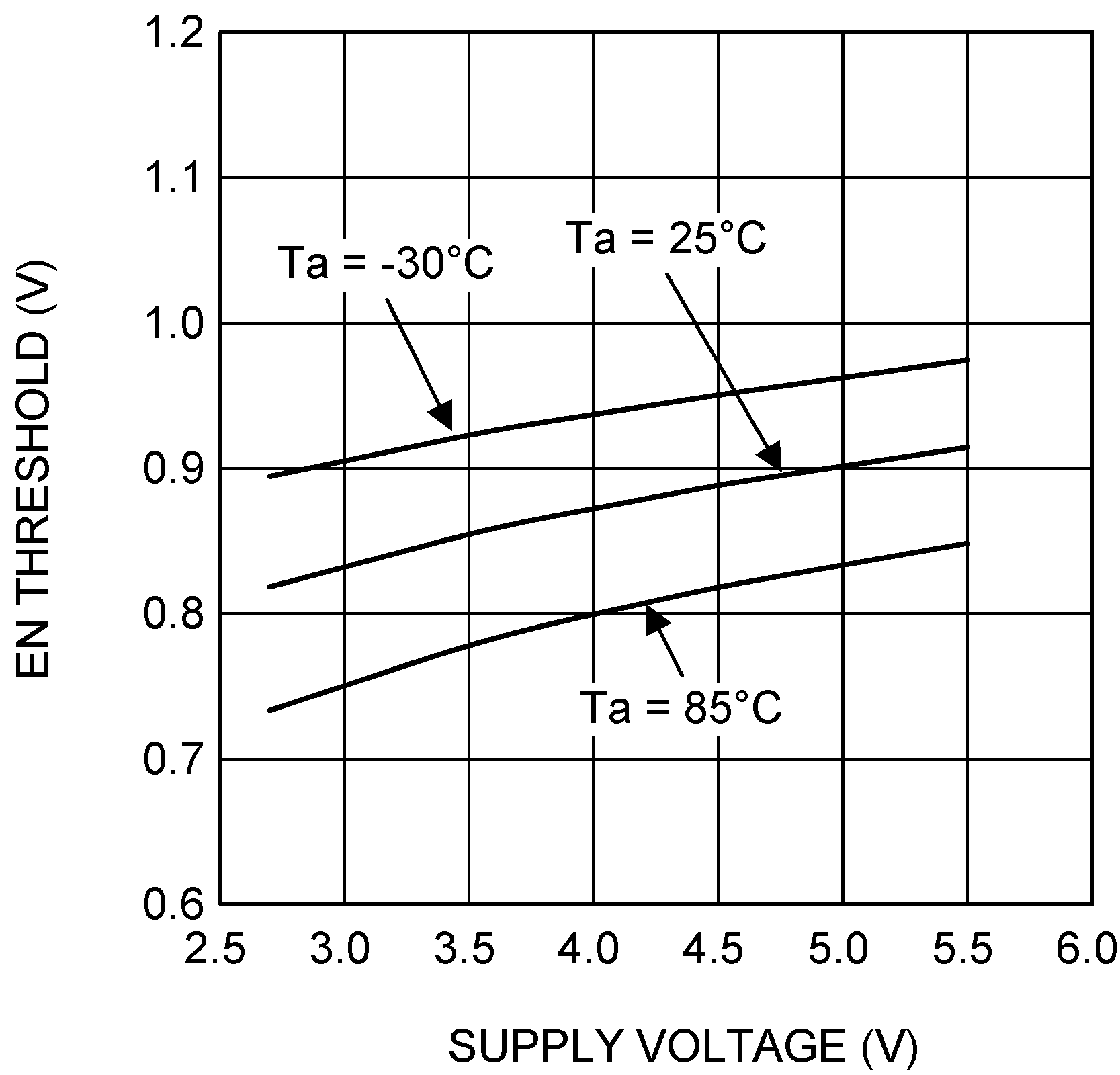
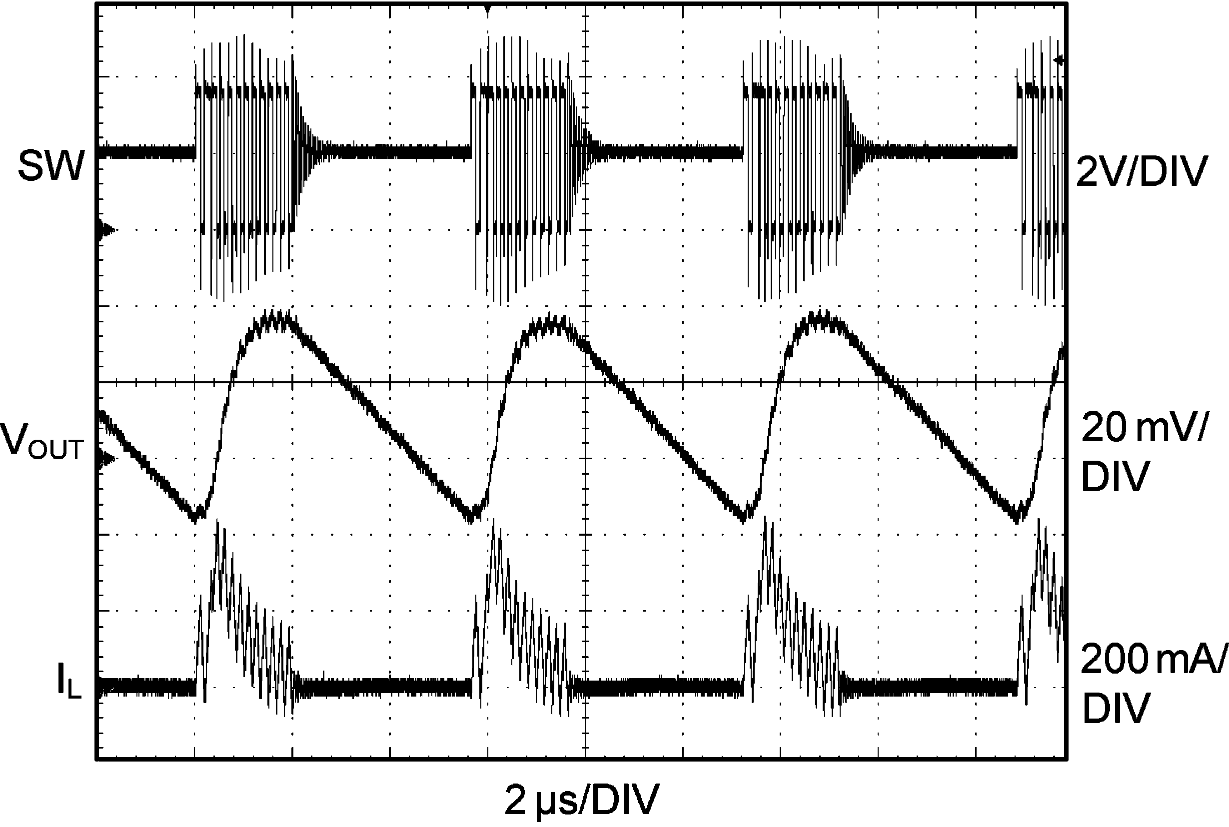
| VOUT = 2 V | IOUT = 50 mA |
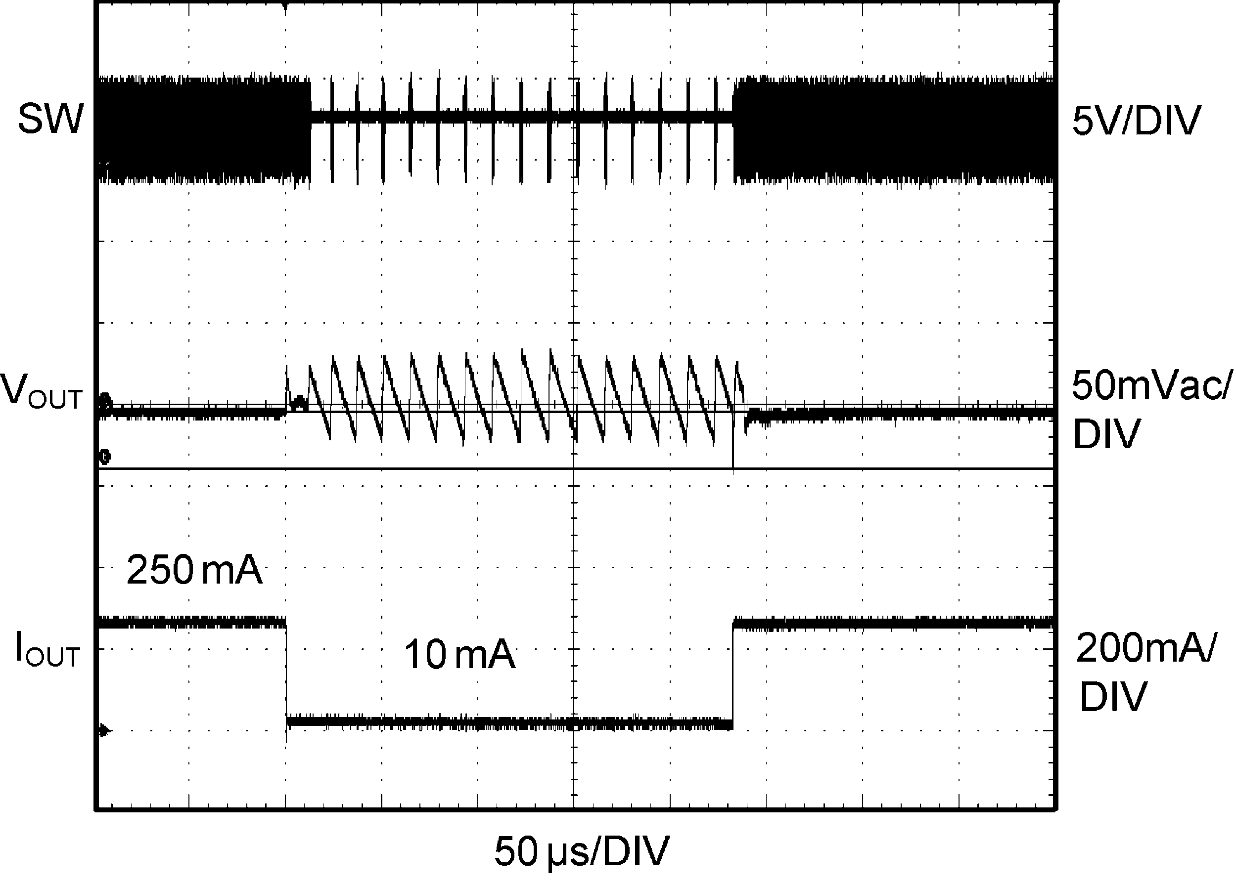
| VOUT = 2.5 V | IOUT = 10 mA/250 mA |
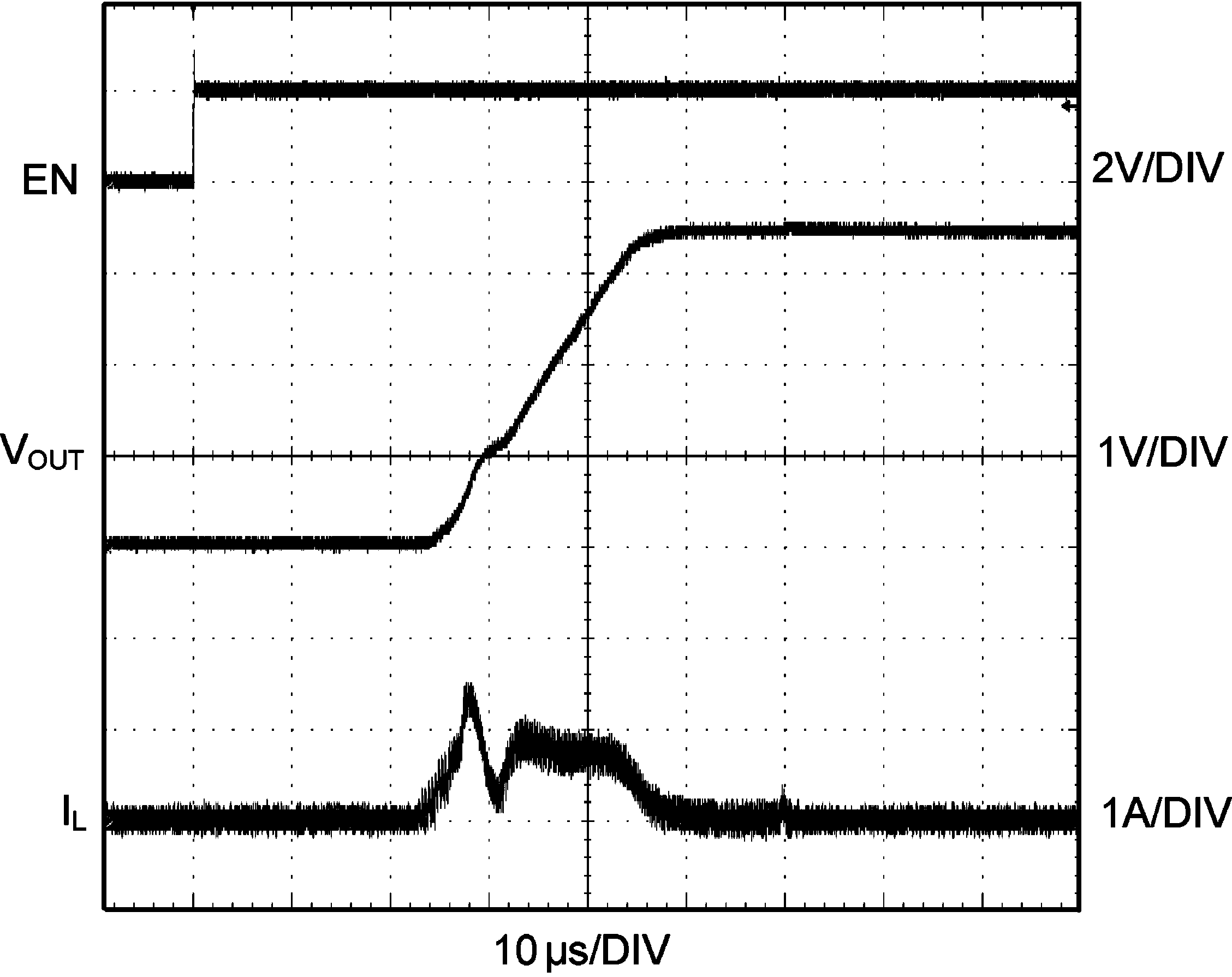
| VIN = 4.2 V | VOUT = 3.4 V | RLOAD = 3.6 kΩ |
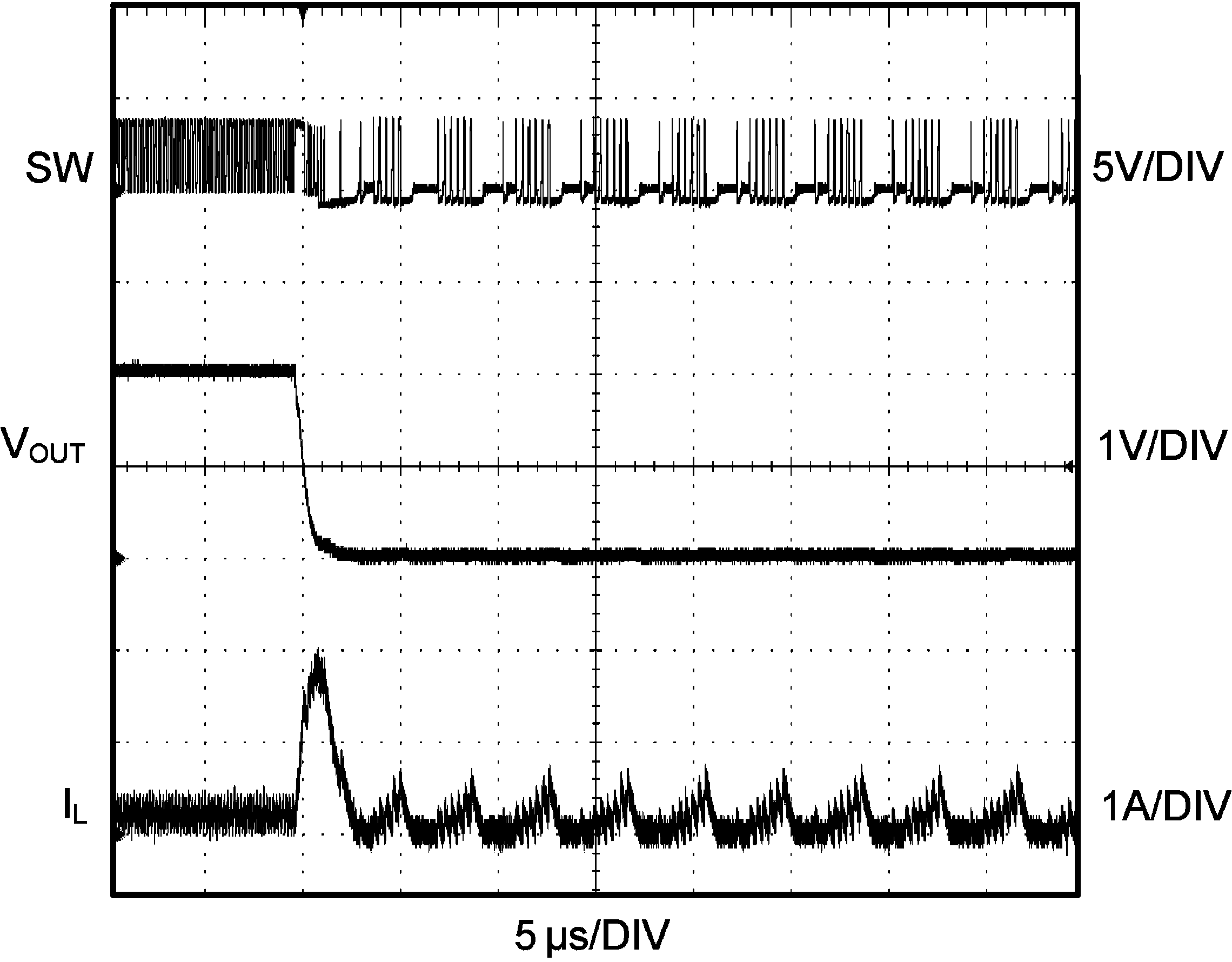
| VOUT = 2 V | RLOAD = 10 Ω |
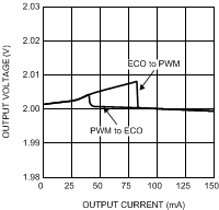
| VOUT = 2 V |
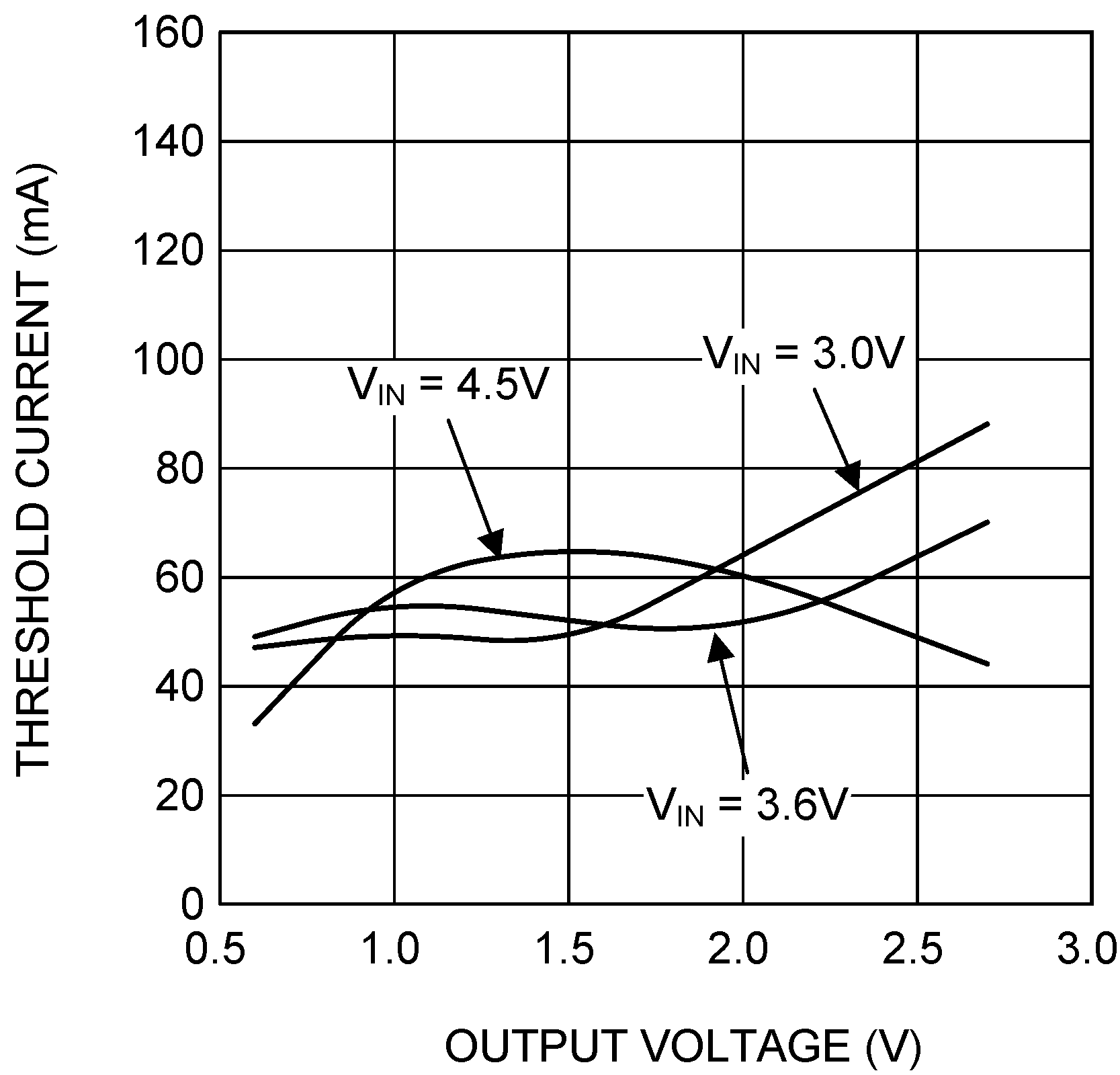
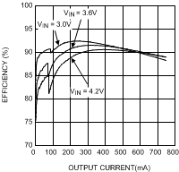
| VOUT = 2 V |
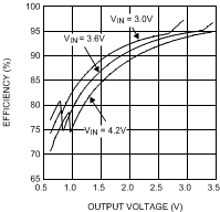
| RLOAD = 10 Ω |
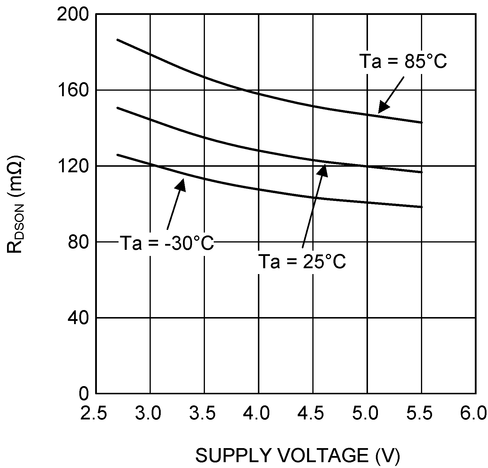
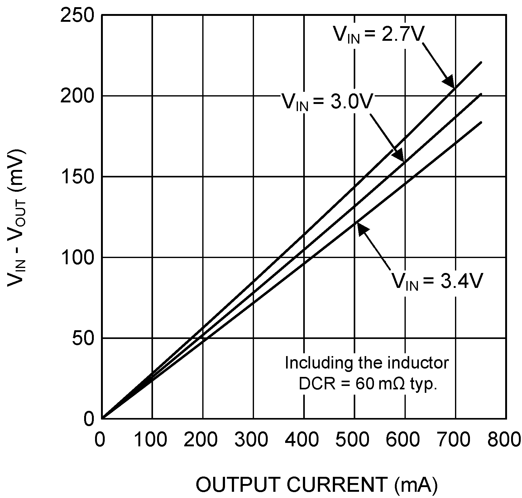
| 100% Duty Cycle |
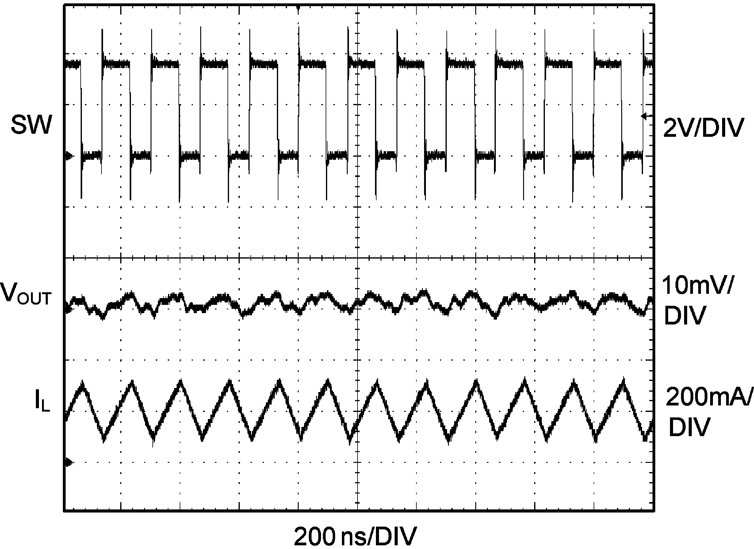
| VOUT = 2 V | IOUT = 200 mA |
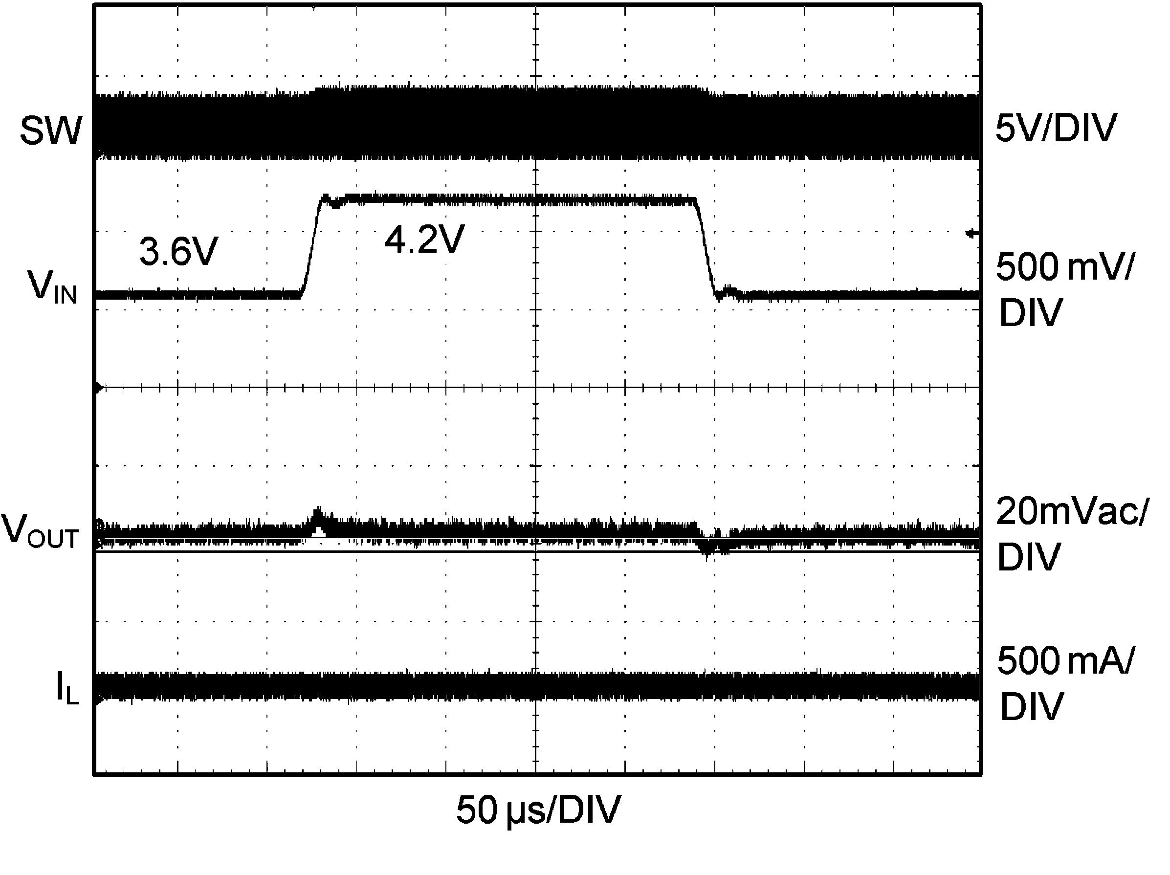
| VIN = 3.6 V/4.2 V | VOUT = 0.8 V | RLOAD = 8 Ω |
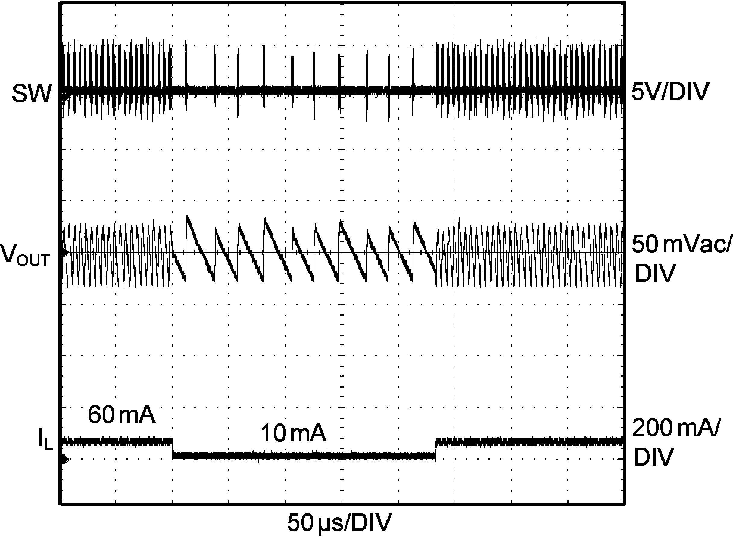
| VOUT = 0.6 V | IOUT = 10 mA/60 mA |
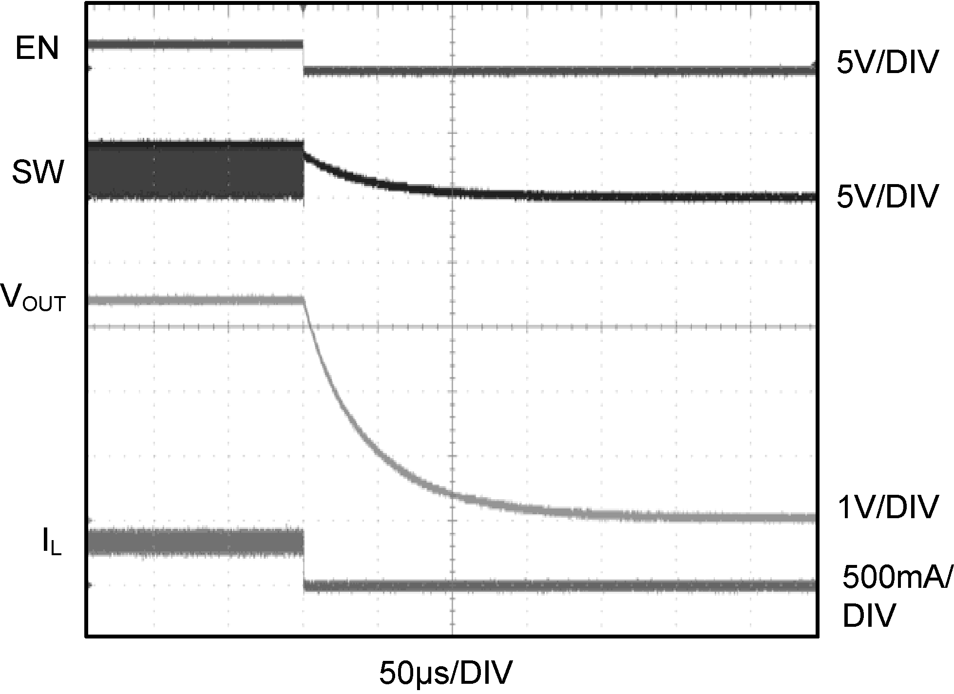
| VIN = 4.2 V | VOUT = 3.4 V | RLOAD = 10 kΩ |