JAJSBC5E May 1998 – December 2016 LM337L
PRODUCTION DATA.
- 1 特長
- 2 アプリケーション
- 3 概要
- 4 改訂履歴
- 5 Pin Configuration and Functions
- 6 Specifications
- 7 Detailed Description
- 8 Application and Implementation
- 9 Power Supply Recommendations
- 10Layout
- 11デバイスおよびドキュメントのサポート
- 12メカニカル、パッケージ、および注文情報
パッケージ・オプション
メカニカル・データ(パッケージ|ピン)
サーマルパッド・メカニカル・データ
発注情報
6 Specifications
6.1 Absolute Maximum Ratings
See (1)(2)| MIN | MAX | UNIT | |
|---|---|---|---|
| Input-output voltage differential | 40 | V | |
| Power dissipation | Internally Limited | ||
| Storage temperature, Tstg | –55 | 150 | °C |
(1) Stresses beyond those listed under Absolute Maximum Ratings may cause permanent damage to the device. These are stress ratings only, which do not imply functional operation of the device at these or any other conditions beyond those indicated under Recommended Operating Conditions. Exposure to absolute-maximum-rated conditions for extended periods may affect device reliability.
(2) If Military/Aerospace specified devices are required, please contact the Texas Instruments Sales Office/Distributors for availability and specifications.
6.2 ESD Ratings
| VALUE | UNIT | |||
|---|---|---|---|---|
| V(ESD) | Electrostatic discharge | Human-body model (HBM), per ANSI/ESDA/JEDEC JS-001(1)(2) | ±1500 | V |
(1) JEDEC document JEP155 states that 500-V HBM allows safe manufacturing with a standard ESD control process. Pins listed as ±1500 V may actually have higher performance.
(2) Human-body model, 1.5k Ω in series with 100 pF.
6.3 Recommended Operating Conditions
over operating free-air temperature range (unless otherwise noted)| MIN | MAX | UNIT | ||
|---|---|---|---|---|
| Operating junction temperature | –25 | 125 | °C | |
6.4 Thermal Information
| THERMAL METRIC(1) | LM337L | UNIT | ||
|---|---|---|---|---|
| D (SOIC) | LP (TO-92) | |||
| 8 PINS | 3 PINS | |||
| RθJA | Junction-to-ambient thermal resistance | 111.3 | 156.9 | °C/W |
| RθJC(top) | Junction-to-case (top) thermal resistance | 56.1 | 80.2 | °C/W |
| RθJB | Junction-to-board thermal resistance | 51.9 | — | °C/W |
| ψJT | Junction-to-top characterization parameter | 10.6 | 24.7 | °C/W |
| ψJB | Junction-to-board characterization parameter | 51.3 | 136.2 | °C/W |
(1) For more information about traditional and new thermal metrics, see the Semiconductor and IC Package Thermal Metrics application report.
6.5 Electrical Characteristics(1)
| PARAMETER | TEST CONDITIONS | MIN | TYP | MAX | UNIT |
|---|---|---|---|---|---|
| Line regulation(2) | TA = 25°C, 3 V ≤ |VIN – VOUT| ≤ 40 V | 0.01 | 0.04 | %/V | |
| Load regulation(2) | TA = 25°C, 5 mA ≤ IOUT ≤ IMAX | 0.1% | 0.5% | ||
| Thermal regulation | TA = 25°C, 10-ms Pulse | 0.04 | 0.2 | %/W | |
| Adjustment pin current | 50 | 100 | μA | ||
| Adjustment pin current change | 5 mA ≤ IL ≤ 100 mA, 3 V ≤ |VIN – VOUT| ≤ 40 V | 0.2 | 5 | μA | |
| Reference voltage | 3 V ≤ |VIN – VOUT| ≤ 40 V, 10 mA ≤ IOUT ≤ 100 mA, P ≤ 625 mW | 1.2 | 1.25 | 1.3 | V |
| Line regulation(2) | 3 V ≤ |VIN – VOUT| ≤ 40 V | 0.02 | 0.07 | %/V | |
| Load regulation(2) | 5 mA ≤ IOUT ≤ 100 mA | 0.3% | 1.5% | ||
| Temperature stability | TMIN ≤ Tj ≤ TMAX | 0.65% | |||
| Minimum load current | |VIN – VOUT| ≤ 40 V | 3.5 | 5 | mA | |
| 3 V ≤ |VIN – VOUT| ≤ 15 V | 2.2 | 3.5 | mA | ||
| Current limit | 3 V ≤ |VIN – VOUT| ≤ 13 V | 100 | 200 | 320 | mA |
| |VIN – VOUT| = 40 V | 25 | 50 | 120 | mA | |
| RMS output noise, % of VOUT | TA = 25°C, 10 Hz ≤ f ≤ 10 kHz | 0.003% | |||
| Ripple rejection ratio | VOUT = –10 V, F = 120 Hz, CADJ = 0 | 65 | dB | ||
| CADJ = 10 μF | 66 | 80 | dB | ||
| Long-term stability | TA = 125°C | 0.3% | 1% |
(1) Unless otherwise specified, these specifications apply –25°C ≤ TJ ≤ 125°C for the LM337L; |VIN – VOUT| = 5 V and IOUT = 40 mA. Although power dissipation is internally limited, these specifications are applicable for power dissipations up to 625 mW. IMAX is 100 mA.
(2) Regulation is measured at constant junction temperature, using pulse testing with a low duty cycle. Changes in output voltage due to heating effects are covered under the specification for thermal regulation.
6.6 Typical Characteristics
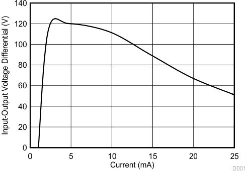
 Figure 1. Current Limit
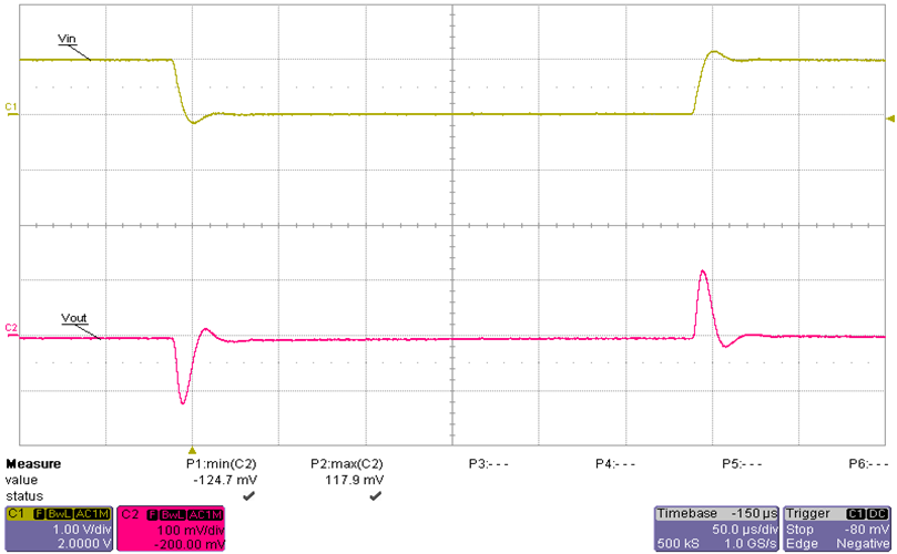
 Figure 3. Line Transient Response
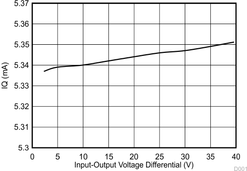
 Figure 2. Minimum Operating Current
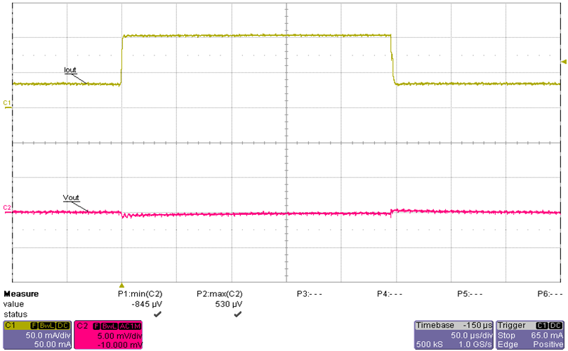
 Figure 4. Load Transient Response