SNVSB96 July 2019 LM3424-Q1
PRODUCTION DATA.
- 1 Features
- 2 Applications
- 3 Description
- 4 Revision History
- 5 Pin Configuration and Functions
- 6 Specifications
-
7 Detailed Description
- 7.1 Overview
- 7.2 Functional Block Diagram
- 7.3
Feature Description
- 7.3.1 Current Regulators
- 7.3.2 Peak Current Mode Control
- 7.3.3 Average LED Current
- 7.3.4 Thermal Foldback and Analog Dimming
- 7.3.5 Current Sense and Current Limit
- 7.3.6 Slope Compensation
- 7.3.7 Control Loop Compensation
- 7.3.8 Start-Up Regulator and Soft-Start
- 7.3.9 Overvoltage Lockout (OVLO)
- 7.3.10 Input Undervoltage Lockout (UVLO)
- 7.3.11 PWM Dimming
- 7.3.12 Thermal Shutdown
- 7.4 Device Functional Modes
-
8 Application and Implementation
- 8.1 Application Information
- 8.2
Typical Applications
- 8.2.1
Basic Topology Schematics
- 8.2.1.1 Design Requirements
- 8.2.1.2
Detailed Design Procedure
- 8.2.1.2.1 Operating Point
- 8.2.1.2.2 Switching Frequency
- 8.2.1.2.3 Average LED Current
- 8.2.1.2.4 Thermal Foldback
- 8.2.1.2.5 Inductor Ripple Current
- 8.2.1.2.6 LED Ripple Current
- 8.2.1.2.7 Peak Current Limit
- 8.2.1.2.8 Slope Compensation
- 8.2.1.2.9 Loop Compensation
- 8.2.1.2.10 Input Capacitance
- 8.2.1.2.11 NFET
- 8.2.1.2.12 Diode
- 8.2.1.2.13 Output OVLO
- 8.2.1.2.14 Input UVLO
- 8.2.1.2.15 Soft-Start
- 8.2.1.2.16 PWM Dimming Method
- 8.2.1.2.17 Analog Dimming Method
- 8.2.2
Buck-Boost Application
- 8.2.2.1 Design Requirements
- 8.2.2.2
Detailed Design Procedure
- 8.2.2.2.1 Operating Point
- 8.2.2.2.2 Switching Frequency
- 8.2.2.2.3 Average LED Current
- 8.2.2.2.4 Thermal Foldback
- 8.2.2.2.5 Inductor Ripple Current
- 8.2.2.2.6 Output Capacitance
- 8.2.2.2.7 Peak Current Limit
- 8.2.2.2.8 Slope Compensation
- 8.2.2.2.9 Loop Compensation
- 8.2.2.2.10 Input Capacitance
- 8.2.2.2.11 NFET
- 8.2.2.2.12 Diode
- 8.2.2.2.13 Input UVLO
- 8.2.2.2.14 Output OVLO
- 8.2.2.2.15 Soft-Start
- 8.2.2.3 Application Curve
- 8.2.3 Boost Application
- 8.2.4 Buck-Boost Application
- 8.2.5 Boost Application
- 8.2.6 Buck-Boost Application
- 8.2.7 Buck Application
- 8.2.8 Buck-Boost Application
- 8.2.9 SEPIC Application
- 8.2.1
Basic Topology Schematics
- 9 Power Supply Recommendations
- 10Layout
- 11Device and Documentation Support
- 12Mechanical, Packaging, and Orderable Information
7.3.4 Thermal Foldback and Analog Dimming
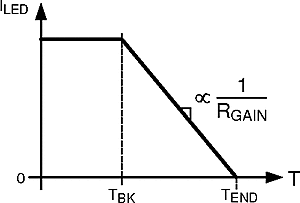
Thermal foldback is necessary in many applications due to the extreme temperatures created in LED environments. In general, two functions are necessary: a temperature breakpoint (TBK) after which the nominal operating current needs to be reduced, and a slope corresponding to the amount of LED current decrease per temperature increase as shown in Figure 19. The LM3424-Q1 allows the user to program both the breakpoint and slope of the thermal foldback profile.
 Figure 19. Ideal Thermal Foldback Profile
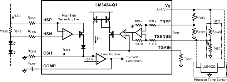
  Figure 20. Thermal Foldback Circuitry
 Foldback is accomplished by adding current (ITF) to the CSH summing node. As more current is added, less current is needed from the high side amplifier and correspondingly, the LED current is regulated to a lower value. The final temperature (TEND) is reached when ITF = ICSH causing no current to be needed from the high-side amplifier, yielding ILED = 0A.
Figure 20 shows how the thermal foldback circuitry is physically implemented in the system. ITF is set by placing a differential voltage (VDIF = VTREF – VTSENSE) across TSENSE and TREF. VTREF can be set with a simple resistor divider (RREF1 and RREF2) supplied from the VS voltage reference (typical 2.45V). VTSENSE is set with a temperature dependant voltage (as temperature increases, voltage should decrease).
An NTC thermistor is the most cost effective device used to sense temperature. As the temperature of the thermistor increases, its resistance decreases (albeit non-linearly). Usually, the NTC manufacturer's datasheet will detail the resistance-temperature characteristic of the thermistor. The thermistor will have a different resistance (RNTC) at each temperature. The nominal resistance of an NTC is the resistance when the temperature is 25°C (R25) and in many datasheets this will be given a multiplier of 1. Then the resistance at a higher temperature will have a multiplier less than 1 (that is, R85 multiplier is 0.161 therefore R85 = 0.161 x R25). Given a desired TBK and TEND, the corresponding resistances at those temperatures (RNTC-BK and RNTC-END) can be found.
Using the NTC method, a resistor divider from VS can be implemented with a resistor connected between VS and TSENSE and the NTC thermistor placed at the desired location and connected from TSENSE to GND. This will ensure that the desired temperature-voltage characteristic occurs at TSENSE.
If a linear decrease over the foldback range is necessary, a precision temperature sensor such as the LM94022 can be used instead as shown in . Either method can be used to set VTSENSE according to the temperature. However, for the rest of this datasheet, the NTC method will be used for thermal foldback calculations.
During operation, if VDIF < 0V, then the sensed temperature is less than TBK and the differential sense amplifier will regulate its output to zero forcing ITF = 0. This maintains the nominal LED current and no foldback is observed.
At TBK, VDIF = 0V exactly and ITF is still zero. Looking at the manufacturer's datasheet for the NTC thermistor, RNTC-BK can be obtained for the desired TBK and the voltage relationship at the breakpoint (VTSENSE-BK = VTREF) can be defined:

A general rule of thumb is to set RREF1 = RREF2 simplifying the breakpoint relationship to RBIAS = RNTC-BK.
If VDIF > 0V (temperature is above TBK), then the amplifier will regulate its output equal to the input forcing VDIF across the resistor (RGAIN) connected from TGAIN to GND. RGAIN ultimately sets the slope of the LED current decrease with respect to increasing temperature by changing ITF:

If an analog temperature sensor such as the LM94022 is used, then RBIAS and the NTC are not necessary and VTSENSE will be the direct voltage output of the sensor.
Since the NTC is not usually local to the controller, a bypass capacitor (CNTC) is suggested from TSENSE to GND. If a capacitor is used at TSENSE, then a capacitor (CREF) of equal or greater value should be placed from TREF to GND in order to ensure the controller does not start-up in foldback. Alternatively, a smaller CREF can be used to create a fade-up function at start-up (see Application Information).
Thermal foldback is simply analog dimming according to a specific profile, therefore any method of controlling the differential voltage between TREF and TSENSE can be use to analog dim the LED current. The corresponding LED current for any VDIF > 0V is defined:

The CSH pin can also be used to analog dim the LED current by adjusting the current sense voltage (VSNS), similar to thermal foldback. There are several different methods to adjust VSNS using the CSH pin:
- External variable resistance: Adjust a potentiometer placed in series with RCSH to vary VSNS.
- External variable current source: Source current (0 µA to ICSH) into the CSH pin to adjust VSNS.
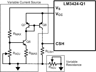
 Figure 21. Analog Dimming Circuitry
 In general, analog dimming applications require a lower switching frequency to minimize the effect of the leading edge blanking circuit. As the LED current is reduced, the output voltage and the duty cycle decreases. Eventually, the minimum on-time is reached. The lower the switching frequency, the wider the linear dimming range. Figure 21 shows how both CSH methods are physically implemented.
Method 1 uses an external potentiometer in the CSH path which is a simple addition to the existing circuitry. However, the LEDs cannot dim completely because there is always some resistance causing signal current to flow. This method is also susceptible to noise coupling at the CSH pin since the potentiometer increases the size of the signal current loop.
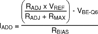
Method 2 provides a complete dimming range and better noise performance, though it is more complex. Like thermal foldback, it simply sources current into the CSH pin, decreasing the amount of signal current that is necessary. This method consists of a PNP current mirror and a bias network consisting of an NPN, 2 resistors and a potentiometer (RADJ), where RADJ controls the amount of current sourced into the CSH pin. A higher resistance value will source more current into the CSH pin causing less regulated signal current through RHSP, effectively dimming the LEDs. Q7 and Q8 should be a dual pair PNP for best matching and performance. The additional current (IADD) sourced into the CSH pin can be calculated:

The corresponding ILED for a specific IADD is:
