JAJSFC4 April 2018 LM3478Q-Q1
PRODUCTION DATA.
- 1 特長
- 2 アプリケーション
- 3 概要
- 4 改訂履歴
- 5 Pin Configuration and Functions
- 6 Specifications
- 7 Detailed Description
-
8 Application and Implementation
- 8.1 Application Information
- 8.2
Typical Applications
- 8.2.1
Typical High Efficiency Step-Up (Boost) Converter
- 8.2.1.1 Design Requirements
- 8.2.1.2
Detailed Design Procedure
- 8.2.1.2.1 Custom Design with WEBENCH Tools
- 8.2.1.2.2 Power Inductor Selection
- 8.2.1.2.3 Programming the Output Voltage
- 8.2.1.2.4 Setting the Current Limit
- 8.2.1.2.5 Current Limit with External Slope Compensation
- 8.2.1.2.6 Power Diode Selection
- 8.2.1.2.7 Power MOSFET Selection
- 8.2.1.2.8 Input Capacitor Selection
- 8.2.1.2.9 Output Capacitor Selection
- 8.2.1.2.10 Compensation
- 8.2.1.3 Application Curves
- 8.2.2 Typical SEPIC Converter
- 8.2.1
Typical High Efficiency Step-Up (Boost) Converter
- 9 Power Supply Recommendations
- 10Layout
- 11デバイスおよびドキュメントのサポート
- 12メカニカル、パッケージ、および注文情報
8.2.1.2.2 Power Inductor Selection
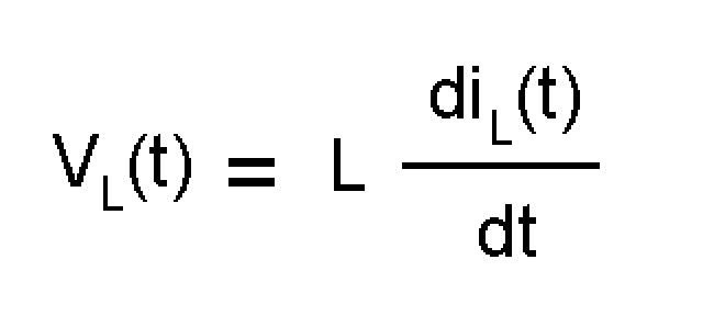
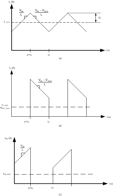
The inductor is one of the two energy storage elements in a boost converter. Figure 29 shows how the inductor current varies during a switching cycle. The current through an inductor is quantified using Equation 10, which shows the relationship of L, IL and VL.

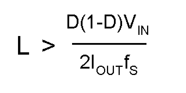
The important quantities in determining a proper inductance value are IL (the average inductor current) and ΔIL (the inductor current ripple). If ΔIL is larger than IL, the inductor current will drop to zero for a portion of the cycle and the converter will operate in the DCM. All the analysis in this datasheet assumes operation in the CCM. To operate in the CCM, the following condition must be met by using Equation 11.

Choose the minimum IOUT to determine the minimum inductance value. A common choice is to set ΔIL to 30% of IL. Choosing an appropriate core size for the inductor involves calculating the average and peak currents expected through the inductor. Use Equation 12, Equation 13, and Equation 14 to the peak inductor current in a boost converter.
An inductor size with ratings higher than these values has to be selected. If the inductor is not properly rated, saturation will occur and may cause the circuit to malfunction.
The LM3478Q-Q1 can be set to switch at very high frequencies. When the switching frequency is high, the converter can be operated with very small inductor values. The LM3478Q-Q1 senses the peak current through the switch which is the same as the peak inductor current as calculated in the previous equation.
 Figure 29. Inductor Current and Diode Current