JAJSAC1H November 2007 – October 2024 LM3481
PRODUCTION DATA
- 1
- 1 特長
- 2 アプリケーション
- 3 概要
- 4 Pin Configuration and Functions
- 5 Specifications
- 6 Detailed Description
-
7 Application and Implementation
- 7.1 Application Information
- 7.2
Typical Applications
- 7.2.1
Boost Converter
- 7.2.1.1 Design Requirements
- 7.2.1.2
Detailed Design Procedure
- 7.2.1.2.1 Custom Design with WEBENCH Tools
- 7.2.1.2.2 Power Inductor Selection
- 7.2.1.2.3 Programming the Output Voltage and Output Current
- 7.2.1.2.4 Current Limit With Additional Slope Compensation
- 7.2.1.2.5 Power Diode Selection
- 7.2.1.2.6 Power MOSFET Selection
- 7.2.1.2.7 Input Capacitor Selection
- 7.2.1.2.8 Output Capacitor Selection
- 7.2.1.2.9 Driver Supply Capacitor Selection
- 7.2.1.2.10 Compensation
- 7.2.1.3 Application Curve
- 7.2.2 Typical SEPIC Converter
- 7.2.1
Boost Converter
- 7.3 Power Supply Recommendations
- 7.4 Layout
- 8 Device and Documentation Support
- 9 Revision History
- 10Mechanical, Packaging, and Orderable Information
5.6 Typical Characteristics
Unless otherwise specified, VIN = 12 V, TJ = 25°C.
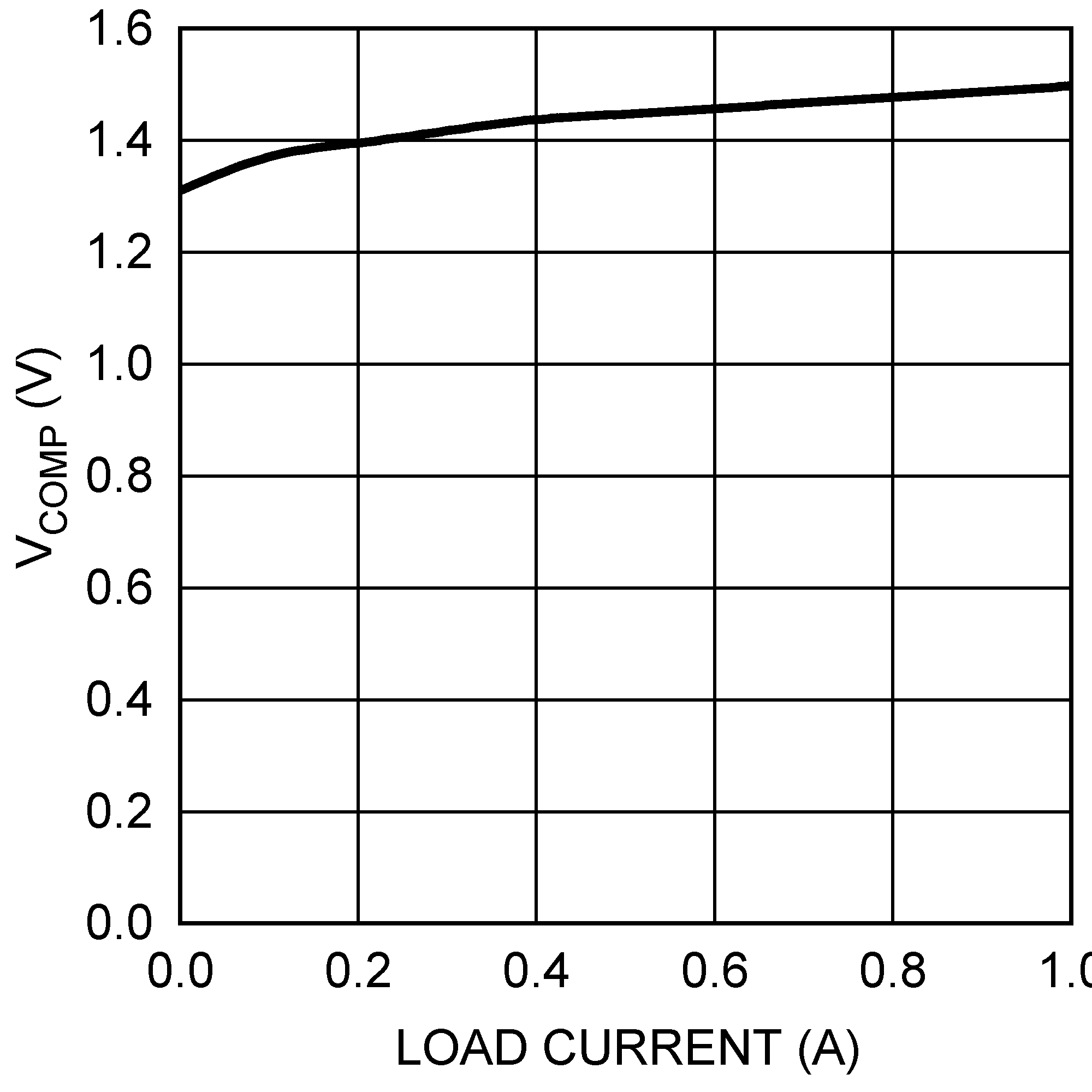 Figure 5-1 Comp Pin Voltage vs. Load Current
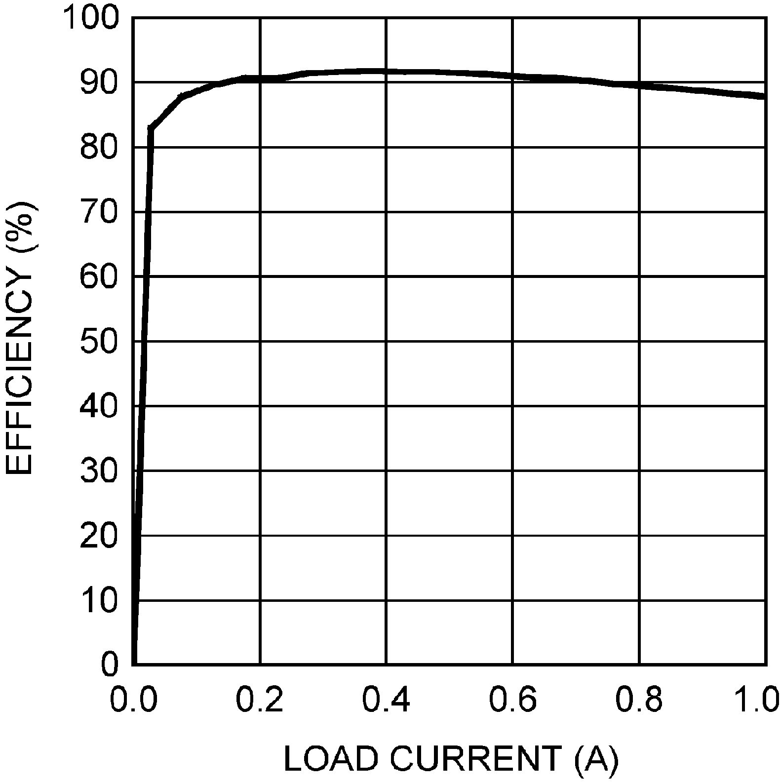 Figure 5-3 Efficiency vs. Load Current (3.3 VIN and 12 VOUT)
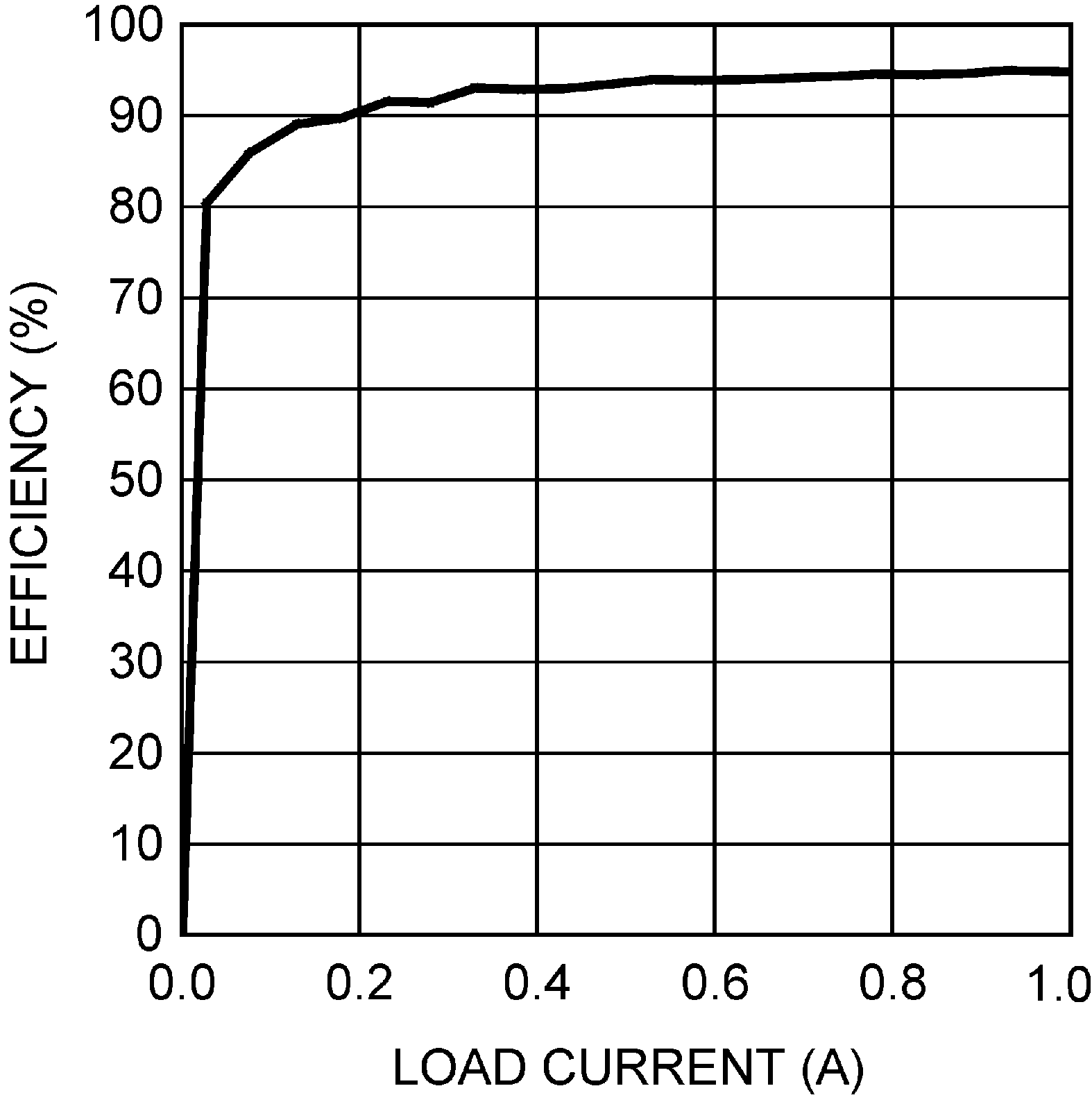 Figure 5-5 Efficiency vs. Load Current (9 VIN and 12 VOUT)
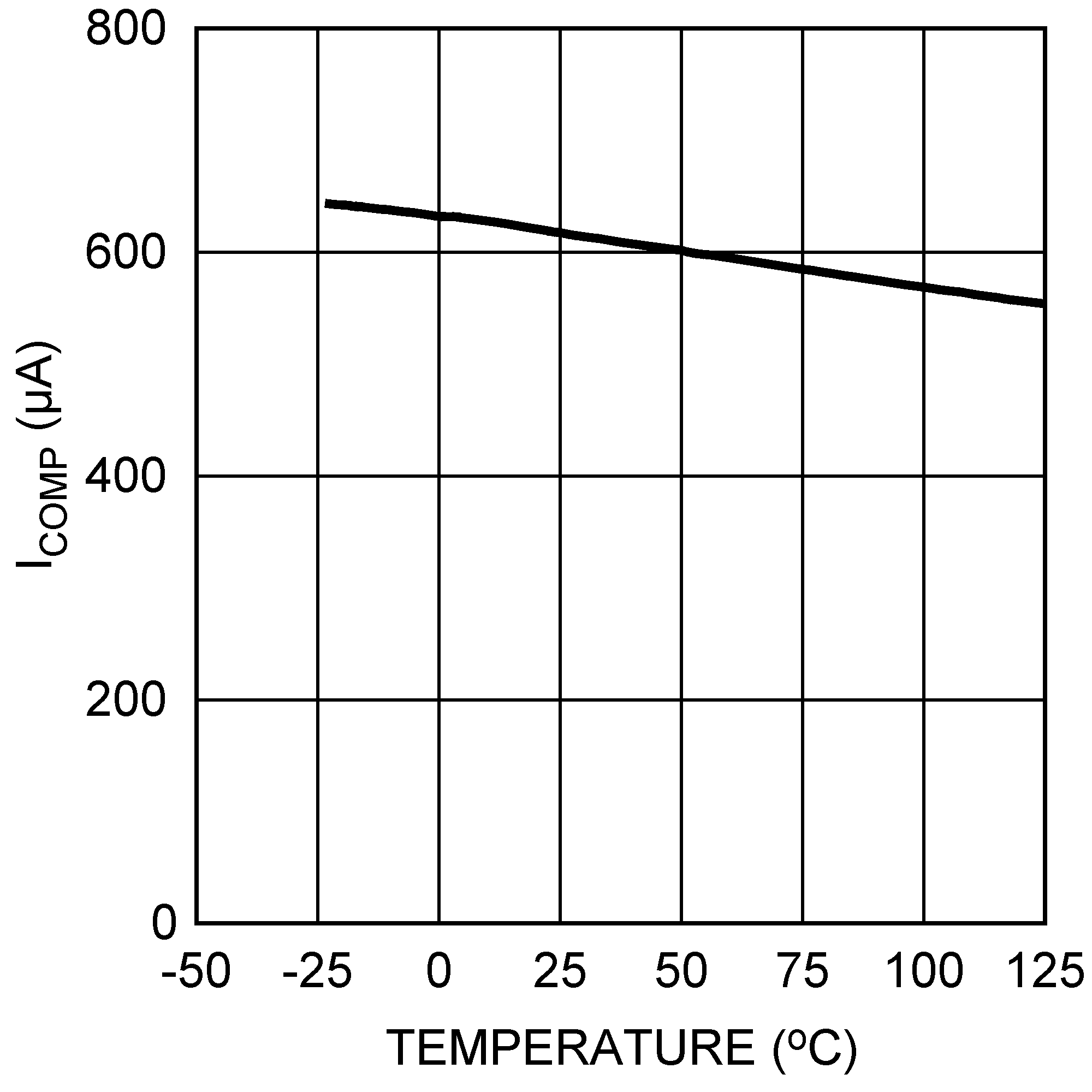 Figure 5-7 COMP Pin Source Current vs. Temperature
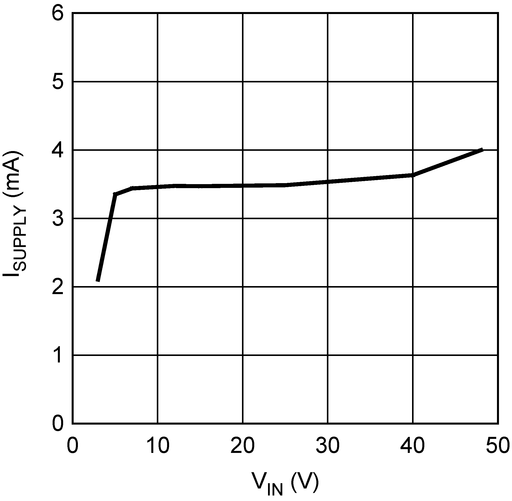 Figure 5-9 ISupply vs. Input Voltage (Switching)
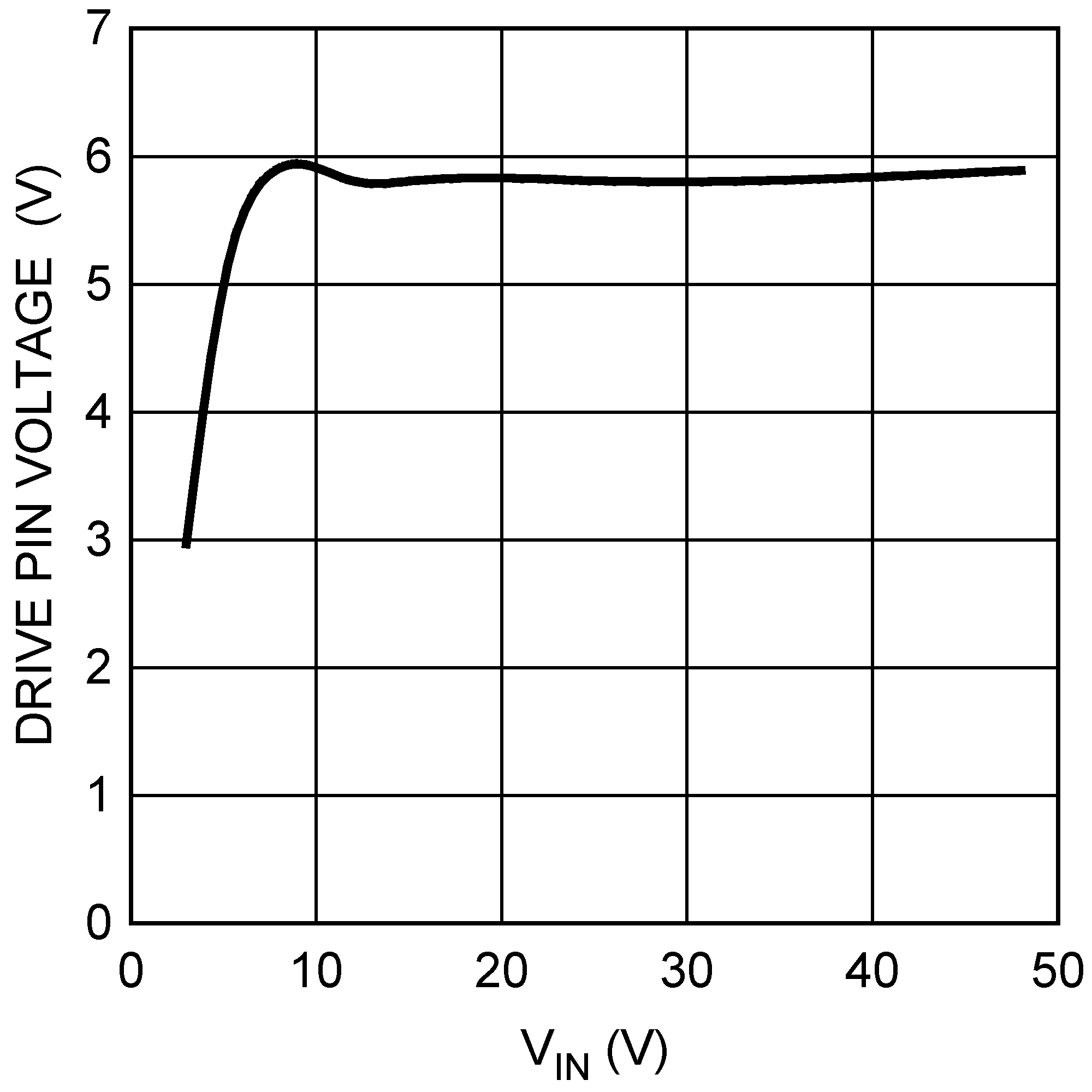 Figure 5-11 Drive Voltage vs. Input Voltage
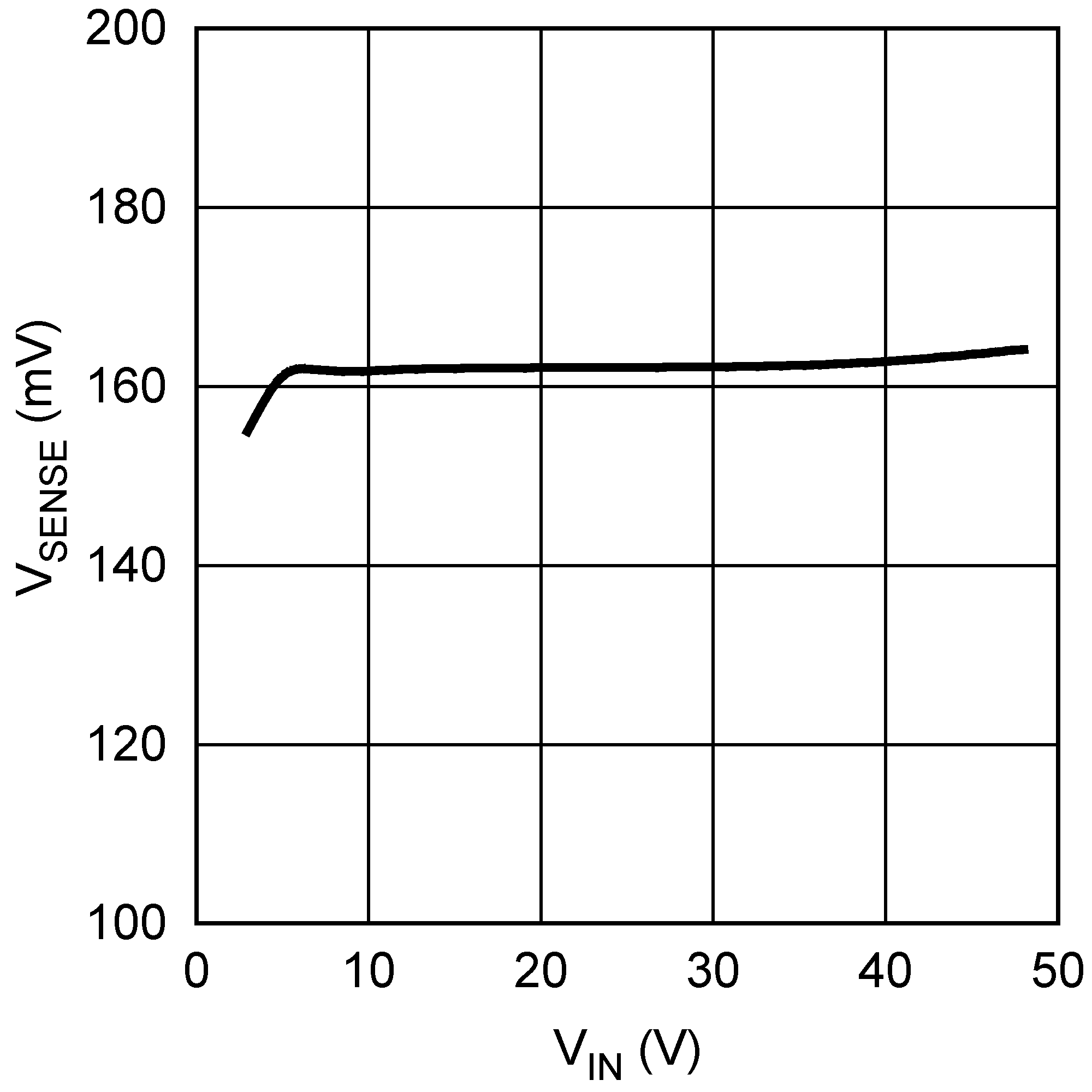 Figure 5-13 Current Sense Threshold vs. Input Voltage
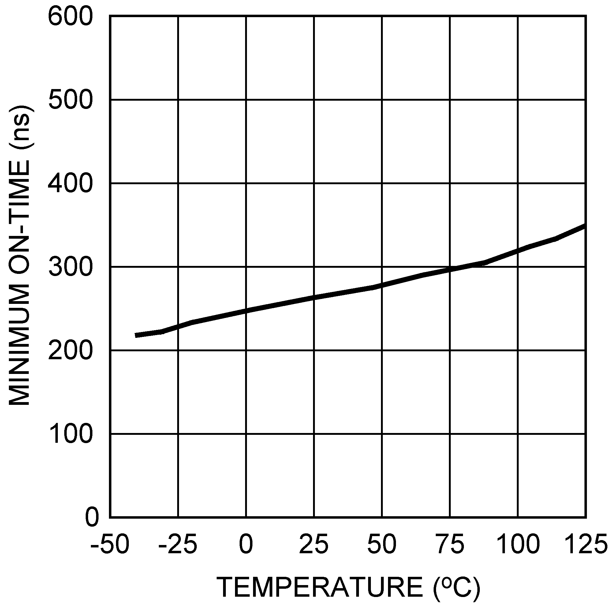 Figure 5-15 Minimum On-Time vs. Temperature
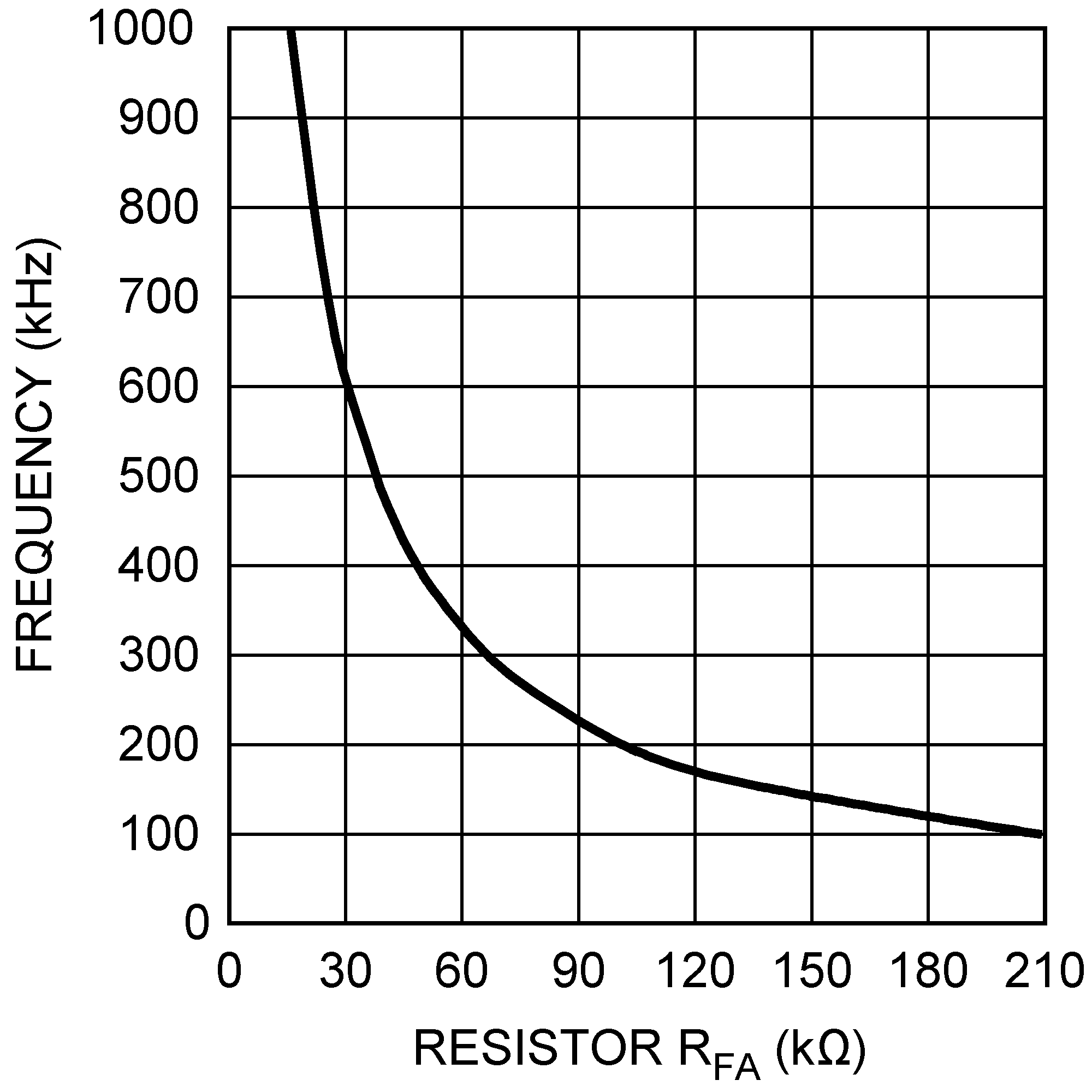 Figure 5-2 Switching Frequency vs. RFA
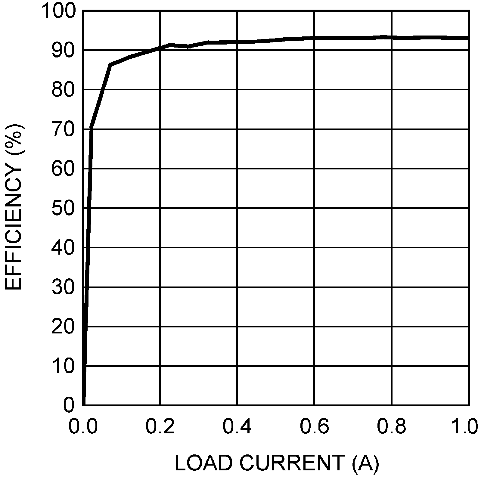 Figure 5-4 Efficiency vs. Load Current (5 VIN and 12 VOUT)
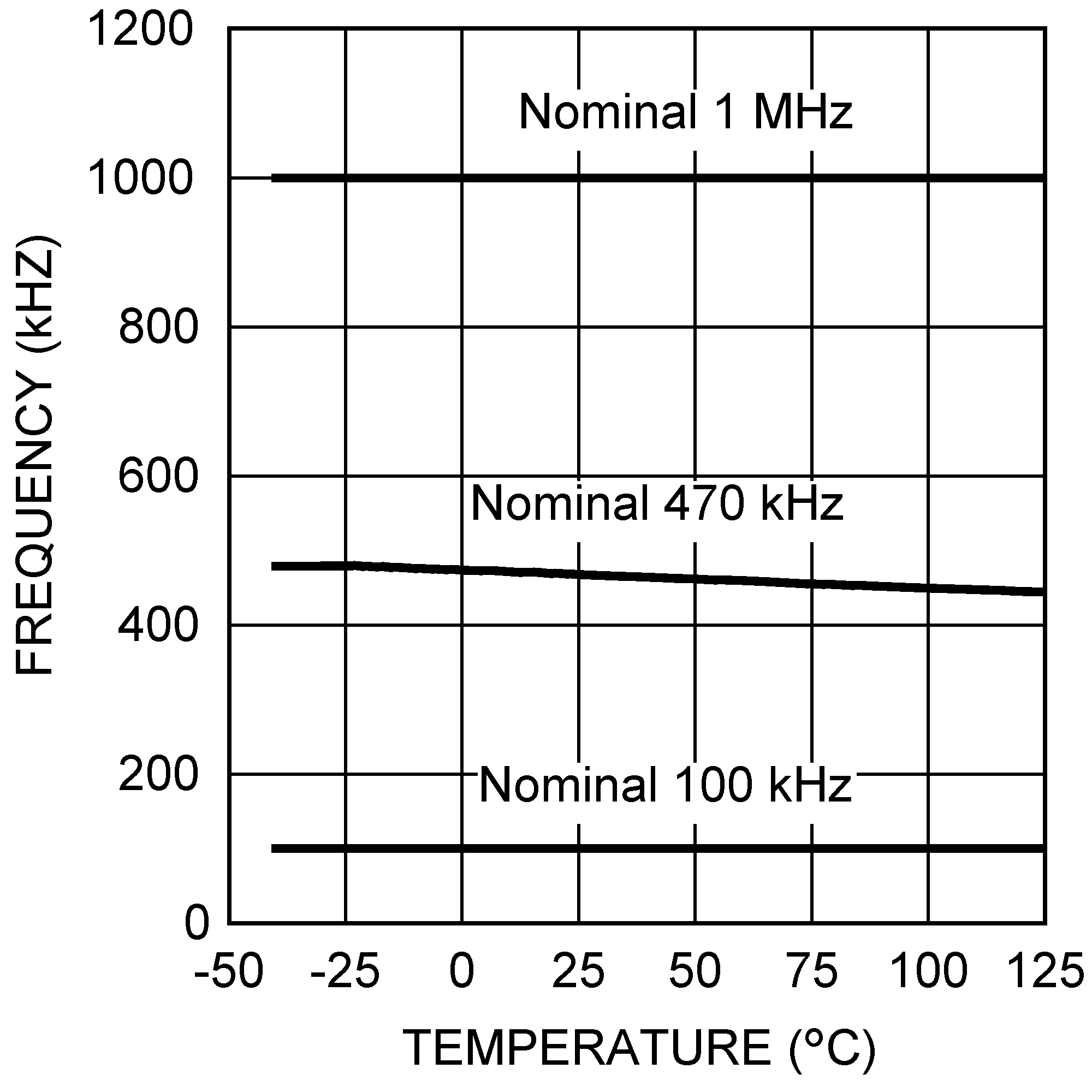 Figure 5-6 Frequency vs. Temperature
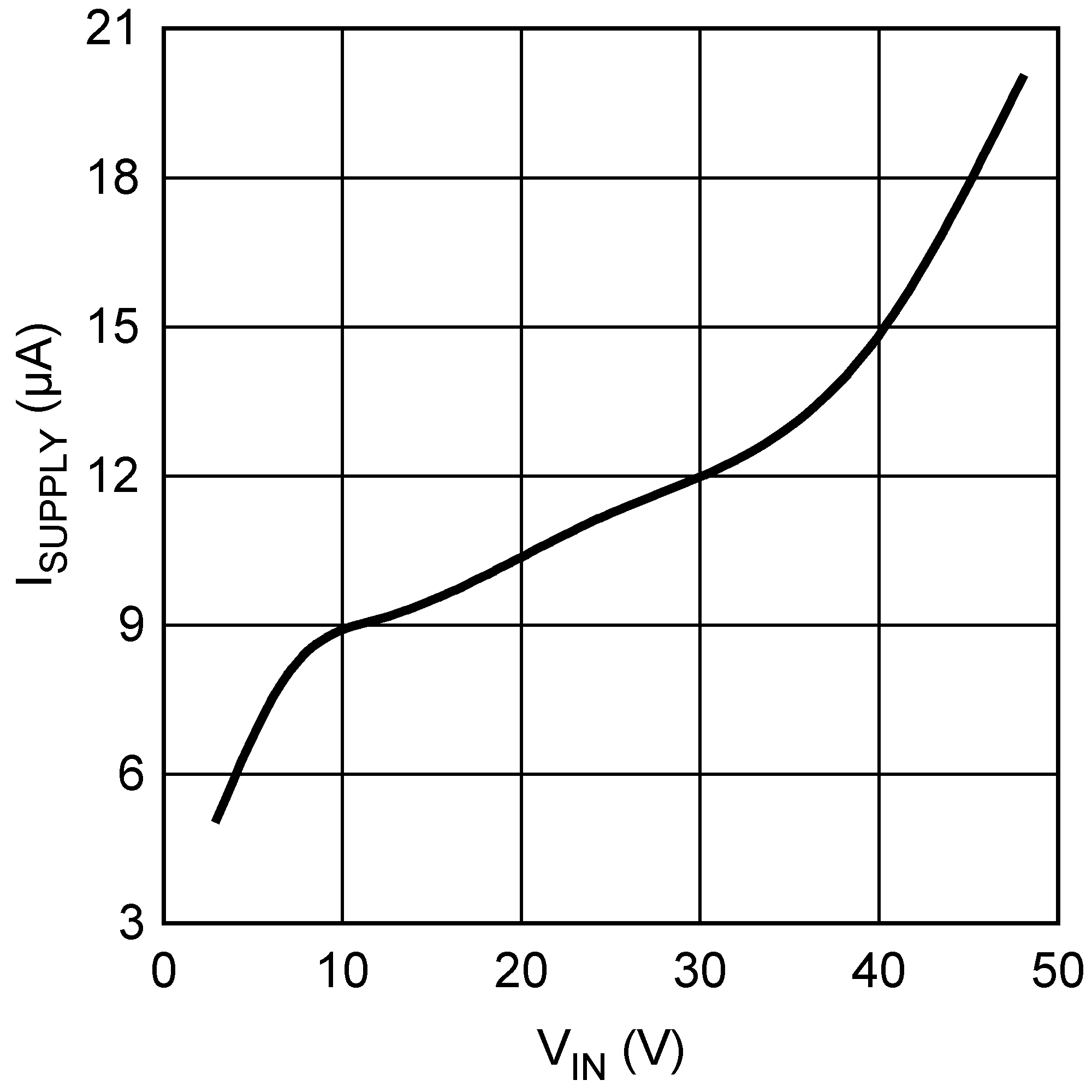 Figure 5-8 ISupplyvs. Input Voltage (Nonswitching)
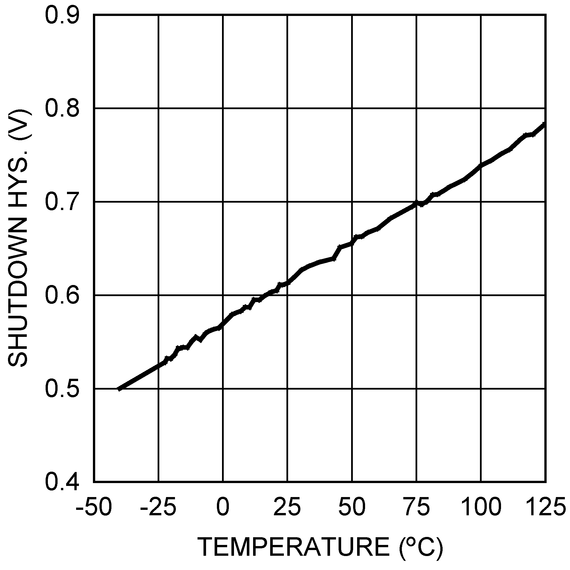 Figure 5-10 Shutdown Threshold Hysteresis vs. Temperature
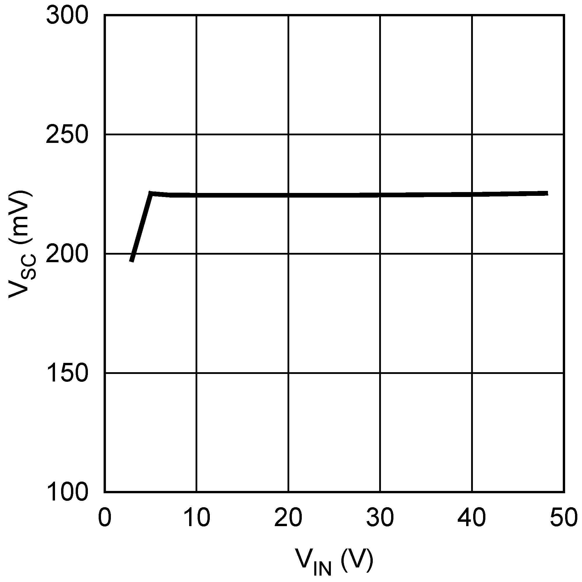 Figure 5-12 Short Circuit Protection vs. VIN
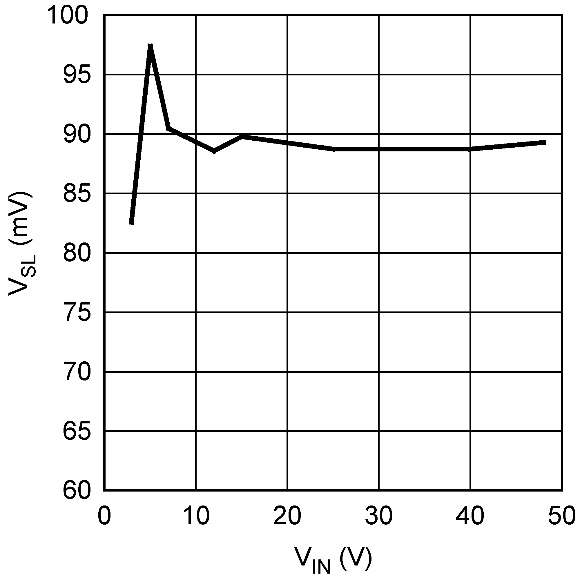 Figure 5-14 Compensation Ramp Amplitude vs. Input Voltage