SNVS797B March 2012 – October 2015 LM3492HC , LM3492HC-Q1
PRODUCTION DATA.
- 1 Features
- 2 Applications
- 3 Description
- 4 Revision History
- 5 Description (continued)
- 6 Pin Configuration and Functions
- 7 Specifications
-
8 Detailed Description
- 8.1 Overview
- 8.2 Functional Block Diagram
- 8.3 Feature Description
- 8.4 Device Functional Modes
- 8.5 Programming
- 9 Application and Implementation
- 10Power Supply Recommendations
- 11Layout
- 12Device and Documentation Support
- 13Mechanical, Packaging, and Orderable Information
パッケージ・オプション
メカニカル・データ(パッケージ|ピン)
- PWP|20
サーマルパッド・メカニカル・データ
- PWP|20
発注情報
7 Specifications
7.1 Absolute Maximum Ratings
over operating free-air temperature range (unless otherwise noted) (1)| MIN | MAX | UNIT | ||
|---|---|---|---|---|
| Input voltage | VIN, RT, VOUT to GND, SW to GND | −0.3 | 67 | V |
| SW to GND (transient <100 ns) | −2 | |||
| Output voltage | ILIM to GND | −0.3 | 1 | V |
| FB to GND | −0.3 | 5 | ||
| COMM, DIM1, DIM2, to GND | −0.3 | 6 | ||
| Junction temperature, TJ | 150 | °C | ||
| Storage temperature, Tstg | –65 | 150 | ||
(1) Stresses beyond those listed under Absolute Maximum Ratings may cause permanent damage to the device. These are stress ratings only, which do not imply functional operation of the device at these or any other conditions beyond those indicated under Recommended Operating Conditions. Exposure to absolute-maximum-rated conditions for extended periods may affect device reliability.
7.2 ESD Ratings
| VALUE | UNIT | |||
|---|---|---|---|---|
| V(ESD) | Electrostatic discharge | Human-body model (HBM), per ANSI/ESDA/JEDEC JS-001(1) | ±2000 | V |
| Charged-device model (CDM), per JEDEC specification JESD22-C101(2) | ±750 | |||
(1) JEDEC document JEP155 states that 500-V HBM allows safe manufacturing with a standard ESD control process. Pins listed as ±2000 V may actually have higher performance.
(2) JEDEC document JEP157 states that 250-V CDM allows safe manufacturing with a standard ESD control process. Pins listed as ±750 V may actually have higher performance.
7.3 Recommended Operating Conditions
over operating free-air temperature range (unless otherwise noted)| MIN | NOM | MAX | UNIT | ||
|---|---|---|---|---|---|
| Supply input voltage, VIN | 4.5 | 65 | V | ||
| Junction temperature, TJ | −40 | 125 | °C | ||
7.4 Thermal Information
| THERMAL METRIC(1) | LM3492HC | UNIT | |
|---|---|---|---|
| PWP (HTSSOP) |
|||
| 20 PINS | |||
| RθJA | Junction-to-ambient thermal resistance | 36.8 | °C/W |
| RθJC(top) | Junction-to-case (top) thermal resistance | 21.8 | °C/W |
| RθJB | Junction-to-board thermal resistance | 18.3 | °C/W |
| ψJT | Junction-to-top characterization parameter | 0.6 | °C/W |
| ψJB | Junction-to-board characterization parameter | 18.1 | °C/W |
| RθJC(bot) | Junction-to-case (bottom) thermal resistance | 2 | °C/W |
(1) For more information about traditional and new thermal metrics, see the Semiconductor and IC Package Thermal Metrics application report, SPRA953.
7.5 Electrical Characteristics
over operating free-air temperature range, VIN = 12 V (unless otherwise noted)| PARAMETER | TEST CONDITIONS | MIN | TYP | MAX | UNIT | |
|---|---|---|---|---|---|---|
| START-UP REGULATOR (VCC PIN) | ||||||
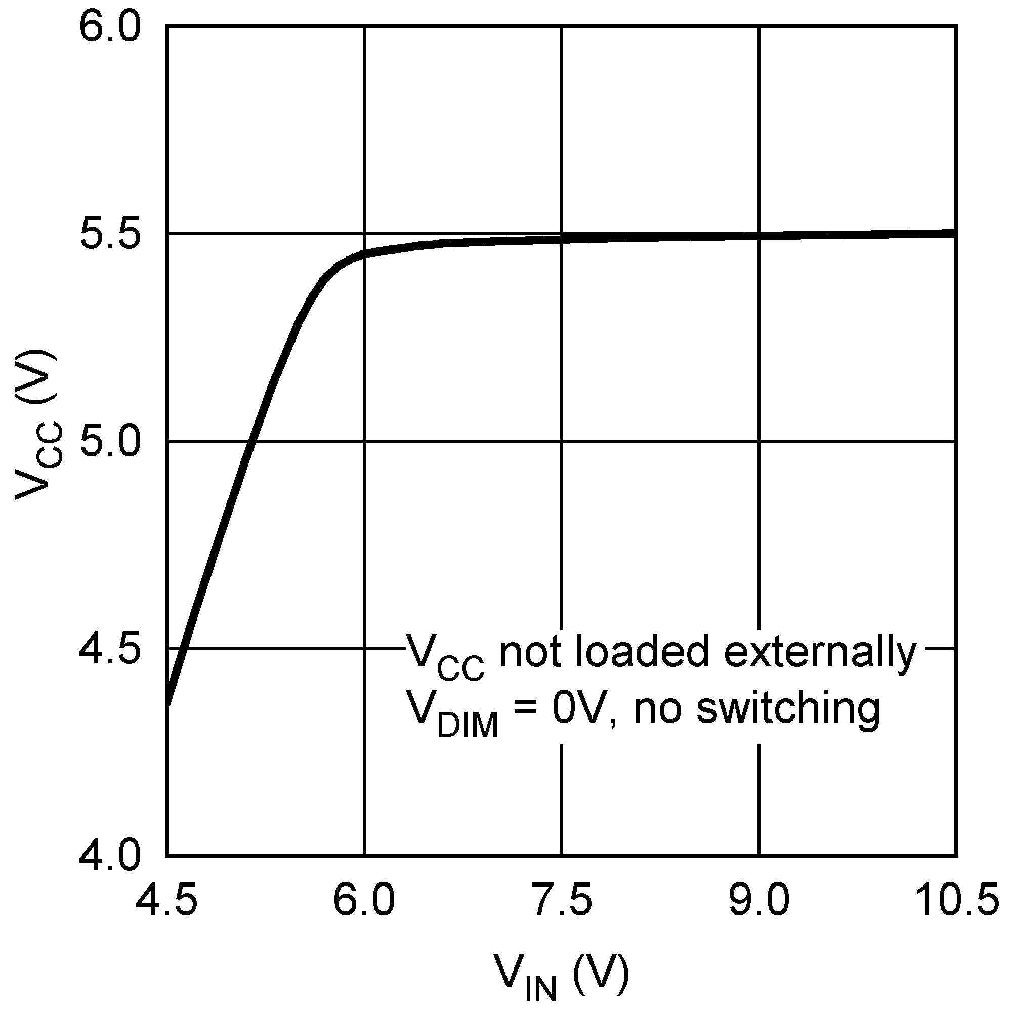
| VVCC | Output voltage | CVCC = 0.47 µF, no load | 4.7 | 5.5 | 6.3 | V |
| IVCC = 2 mA | 4.7 | 5.5 | 6.3 | V | ||
| VCC_UVLO | VCC pin undervoltage lockout threshold (UVLO) | VVCC increasing, TA = TJ = 25°C | 3.56 | 3.78 | 4 | V |
| VCC_UVLO-HYS | VCC pin UVLO hysteresis | VVCC decreasing, TA = TJ = 25°C | 310 | mV | ||
| IIN | IIN operating current | No switching, VFB = 0 V | 3.6 | 5.2 | mA | |
| IIN-SD | IIN operating current, device shutdown | VEN = 0 V | 30 | 95 | µA | |
| IVCC | VCC pin current limit (1) | VVCC = 0 V | 18 | 30 | mA | |
| VCC-VOUT | VCC pin output voltage when supplied by VOUT | VIN = Open, IVCC = 1 mA, VOUT = 18 V |
3.5 | 4.1 | 4.7 | V |
| ENABLE INPUT | ||||||
| VEN | EN pin input threshold | VEN rising | 1.55 | 1.63 | 1.71 | V |
| VEN-HYS | EN pin threshold hysteresis | VEN falling | 194 | mV | ||
| IEN-SHUT | Enable pullup current at shutdown | VEN = 0 V | 2 | µA | ||
| IEN-OPER | Enable pullup current during operation | VEN = 2 V | 40 | µA | ||
| CURRENT REGULATOR | ||||||
| VIREF | IREF pin voltage | 4.5 V ≤ VIN ≤ 65 V | 1.231 | 1.256 | 1.281 | V |
| VDHC50 | VIOUT under DHC | IOUT = 50 mA, RIREF = 25 kΩ | 0.160 | 0.225 | 0.290 | V |
| VDHC100 | IOUT = 100 mA, RIREF = 12.5 kΩ | 0.38 | 0.48 | 0.58 | ||
| VDHC200 | IOUT = 200 mA, RIREF = 6.25 kΩ | 0.81 | 0.99 | 1.17 | ||
| VDHC250 | IOUT = 250 mA, RIREF = 5 kΩ | 0.81 | 1.21 | 1.44 | ||
| IOUT50 | Current output under DHC | VIOUT = VDHC50, RIREF = 25 kΩ, TA = TJ = 25°C |
47.5 | 50 | 52.5 | mA |
| VIOUT = VDHC50, RIREF = 25 kΩ | 46.5 | 50 | 53.5 | |||
| IOUT100 | VIOUT = VDHC100, RIREF = 12.5 kΩ, TA = TJ = 25°C |
97 | 100 | 103 | ||
| VIOUT = VDHC100, RIREF = 12.5 kΩ | 96 | 100 | 104 | |||
| IOUT200 | VIOUT = VDHC200, RIREF = 6.25 kΩ, TA = TJ = 25°C |
194 | 200 | 206 | ||
| VIOUT = VDHC200, RIREF = 6.25 kΩ | 192 | 200 | 208 | |||
| IOUT250 | VIOUT = VDHC250, RIREF = 5 kΩ, TA = TJ = 25°C |
241.3 | 250 | 258.8 | ||
| VIOUT = VDHC250, RIREF = 5 kΩ | 238 | 250 | 262 | |||
| IOUTOFF | Leakage at maximum work voltage | VDIM = 0, VIOUT = 65 V | 5 | µA | ||
| VIOUT50-MIN | Minimum work voltage | IOUT = 50 mA, RIREF = 25 kΩ, IOUT = 0.98 × IOUT50, TA = TJ = 25°C |
0.1 | 0.15 | V | |
| VIOUT100-MIN | IOUT = 100 mA, RIREF = 12.5 kΩ, IOUT = 0.98 × IOUT100, TA = TJ = 25°C |
0.2 | 0.35 | |||
| VIOUT200-MIN | IOUT = 200 mA, RIREF = 6.25 kΩ, IOUT = 0.98 × IOUT200, TA = TJ = 25°C |
0.4 | 0.65 | |||
| VIOUT250-MIN | IOUT = 250 mA, RIREF = 5 kΩ, IOUT = 0.98 × IOUT250, TA = TJ = 25°C |
0.5 | 0.82 | |||
| VDIM-HIGH | DIM voltage HIGH | 1.17 | V | |||
| VDIM-LOW | DIM voltage LOW | 0.7 | V | |||
| BOOST CONVERTER | ||||||
| ICDHC-SRC | CDHC pin source current | VCDHC = 1.6 V, VFB = 3 V, VIOUT = 0 V, DIM = High |
60 | µA | ||
| ICDHC-SINK | CDHC pin sink current | VCDHC = 1.6 V, VFB = 3 V, VIOUT = 3 V, DIM = High |
56 | µA | ||
| ICDHC-PULLUP | CDHC pin pullup current | DIM = Low, VCDHC = 2.3 V, VFB = 3 V |
10 | 200 | 500 | nA |
| ICL-MAX | Integrated MOSFET peak current limit threshold | 3.3 | 3.9 | 4.5 | A | |
| ICL-HALF | Half integrated MOSFET peak current limit threshold | RILIM = 11 kΩ | 2 | A | ||
| RDS(on) | Integrated MOSFET On-resistance | ISW = 500 mA | 0.19 | 0.43 | Ω | |
| VFBTH-PWRGD | Power-Good FB pin threshold | 2.25 | V | |||
| VFB-OVP | FB pin overvoltage protection threshold FB pin OVP hysteresis | VFB rising, VCDHC = 4 V | 2.64 | 2.76 | 2.88 | V |
| VFB falling | 0.1 | 0.215 | 0.323 | |||
| IFB | Feedback pin input current | VFB = 3 V | 1 | µA | ||
| tON | ON timer pulse width | VIN = 12 V, VOUT = 65V, RRT = 300 kΩ |
1460 | ns | ||
| VIN = 24 V, VOUT = 32.5V, RRT = 300 kΩ |
800 | |||||
| VIN = 12 V, VOUT = 65V, RRT = 100 kΩ |
550 | |||||
| VIN = 24 V, VOUT = 32.5V, RRT = 100 kΩ |
350 | |||||
| tON(min)ILIM | ON timer minimum pulse width at current limit | 145 | ns | |||
| tOFF | OFF timer pulse width | 145 | 350 | ns | ||
| COMM PIN | ||||||
| VIOUT-OV | IOUT pin overvoltage threshold | COMM goes LOW during VIOUT rising, other VIOUT = 1.2 V | 5.6 | 6.7 | 7.8 | V |
| VCOMM-LOW | COMM pin at LOW | 5 mA into COMM | 0.7 | V | ||
| ILEAK-FAULT | COMM pin open leakage | VCOMM = 5 V | 5 | µA | ||
| THERMAL PROTECTION | ||||||
| TOTM | Overtemperature indication | TJ rising | 135 | °C | ||
| TOTM-HYS | Over-temperature indication hysteresis | TJ falling | 15 | °C | ||
| TSD | Thermal shutdown temperature | TJ rising | 165 | °C | ||
| TSD-HYS | Thermal shutdown temperature hysteresis | TJ falling | 20 | °C | ||
(1) The VCC pin provides self bias for the internal gate drive and control circuits. Device thermal limitations limit external loading.
7.6 Typical Characteristics
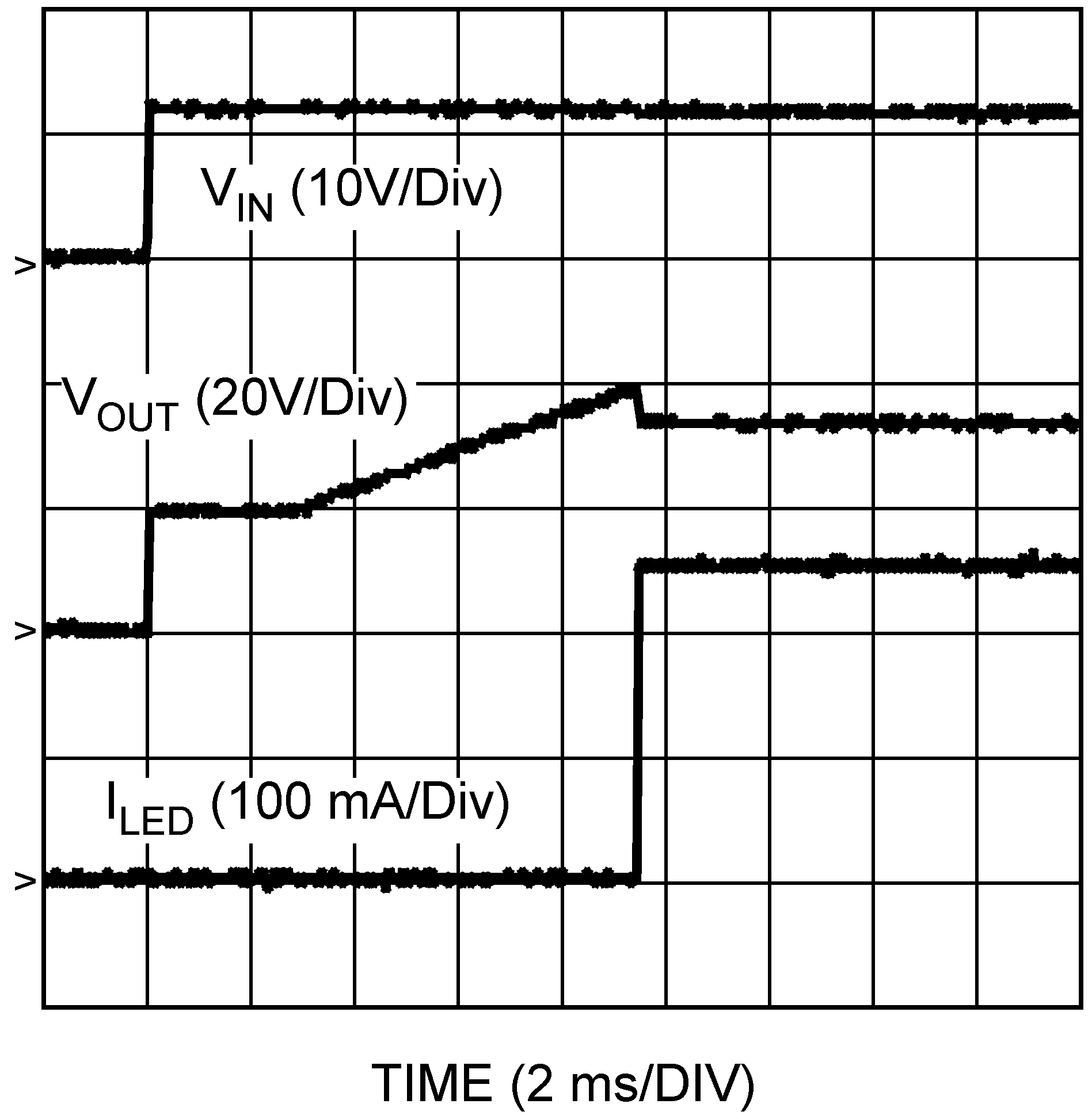
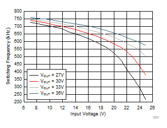
Unless otherwise specified the following conditions apply: TJ = 25°C, VIN = 12 V with configuration in typical application circuit for ILED = 250 mA shown in this data sheet.


| ILED = 0.25 A |

| ILED = 0.25 A |


| ILED = 0.25 A | Dimming frequency = 200 Hz | |

| ILED = 0.15 A | RRT = 178 kΩ |

| ILED = 0.15 A | RRT = 178 kΩ |


| ILED = 0.25 A |

| ILED = 0.25 A |

| ILED = 0.25 A | Dimming frequency = 200 Hz | |

| ILED = 0.25 A | Dimming frequency = 200 Hz | |

| ILED = 0.15 A | RRT = 499 kΩ |

| ILED = 0.15 A | RRT = 499 kΩ |