SNVS653E July 2011 – August 2015 LM3532
PRODUCTION DATA.
- 1 Features
- 2 Applications
- 3 Description
- 4 Revision History
- 5 Pin Configuration and Functions
- 6 Specifications
-
7 Detailed Description
- 7.1 Overview
- 7.2 Functional Block Diagram
- 7.3 Feature Description
- 7.4
Device Functional Modes
- 7.4.1 LED Current Ramping
- 7.4.2 Start-up and Shutdown Current Ramping
- 7.4.3 Run-Time Ramp Rates
- 7.4.4 LED Current Mapping Modes
- 7.4.5 Exponential Current Mapping Mode
- 7.4.6 Linear Current Mapping
- 7.4.7 LED Current Control
- 7.4.8 Assigning and Enabling a PWM Input
- 7.4.9 Enabling a Current Sink
- 7.4.10
Ambient Light Sensor Current Control
- 7.4.10.1 ALS Resistors
- 7.4.10.2 Ambient Light Zone Boundaries
- 7.4.10.3 Ambient Light Zone Hysteresis
- 7.4.10.4 PWM Enabled for a Particular Zone
- 7.4.10.5 ALS Operation
- 7.4.10.6 ALS Input Select and ALS ADC Input
- 7.4.10.7 ALS ADC Readback
- 7.4.10.8 ALS Averaging
- 7.4.10.9 ALS ADC Average Readback
- 7.4.10.10 Initializing the ALS
- 7.4.10.11 ALS Operation
- 7.4.10.12 Direct ALS Control
- 7.4.11 Down Delay
- 7.5 Programming
- 7.6
Register Maps
- 7.6.1 Output Configuration
- 7.6.2 Start-up/Shutdown Ramp Rate
- 7.6.3 Run-Time Ramp Rate
- 7.6.4 Control A PWM
- 7.6.5 Control B PWM
- 7.6.6 Control C PWM
- 7.6.7 Control A Brightness Configuration
- 7.6.8 Control B Brightness Configuration
- 7.6.9 Control C Brightness Configuration
- 7.6.10 Control A, B, and C Full-Scale Current
- 7.6.11 Feedback Enable
- 7.6.12 Control Enable
- 7.6.13 ALS1 and ALS2 Resistor Select
- 7.6.14 ALS Down Delay
- 7.6.15 ALS Configuration
- 7.6.16 ALS Zone Readback / Information
- 7.6.17 ALS Zone Boundaries
- 7.6.18 Zone Target Registers
- 8 Application and Implementation
- 9 Power Supply Recommendations
- 10Layout
- 11Device and Documentation Support
- 12Mechanical, Packaging, and Orderable Information
1 Features
- Drives up to 3 Parallel High-Voltage LED Strings at 40 V Each With up to 90% Efficiency
- 0.4% Typical Current Matching Between Strings
- 256 Level Logarithmic and Linear Brightness Control With 14-Bit Equivalent Dimming
- I2C-Compatible Interface
- Direct Read Back of Ambient Light Sensor Via
8-bit ADC - Programmable Dual Ambient Light Sensor Inputs With Internal Sensor Gain Selection
- Dual External PWM Inputs for LED Brightness Adjustment
- Independent Current String Brightness Control
- Programmable LED Current Ramp Rates
- 40-V Overvoltage Protection
- 1-A Typical Current Limit
2 Applications
- Power Source for White LED Backlit LCD Displays
- Programmable Keypad Backlight
3 Description
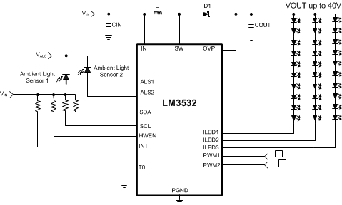
The LM3532 is a 500-kHz fixed frequency asynchronous boost converter which provides the power for 3 high-voltage, low-side current sinks. The device is programmable over an I2C-compatible interface and has independent current control for all three channels. The adaptive current regulation method allows for different LED currents in each current sink thus allowing for a wide variety of backlight and keypad applications.
The main features of the LM3532 include dual ambient light sensor inputs each with 32 internal voltage setting resistors, 8-bit logarithmic and linear brightness control, dual external PWM brightness control inputs, and up to 1000:1 dimming ratio with programmable fade in and fade out settings.
The LM3532 is available in a 16-pin, 0.4-mm pitch thin DSBGA package. The device operates over a 2.7-V to 5.5-V input voltage range and the −40°C to +85°C temperature range.
Device Information(1)
| PART NUMBER | PACKAGE | BODY SIZE (MAX) |
|---|---|---|
| LM3532 | DSBGA (16) | 1.87 mm x 1.77 mm |
- For all available packages, see the orderable addendum at the end of the data sheet.
Typical Application Circuit
