SNVS653E July 2011 – August 2015 LM3532
PRODUCTION DATA.
- 1 Features
- 2 Applications
- 3 Description
- 4 Revision History
- 5 Pin Configuration and Functions
- 6 Specifications
-
7 Detailed Description
- 7.1 Overview
- 7.2 Functional Block Diagram
- 7.3 Feature Description
- 7.4
Device Functional Modes
- 7.4.1 LED Current Ramping
- 7.4.2 Start-up and Shutdown Current Ramping
- 7.4.3 Run-Time Ramp Rates
- 7.4.4 LED Current Mapping Modes
- 7.4.5 Exponential Current Mapping Mode
- 7.4.6 Linear Current Mapping
- 7.4.7 LED Current Control
- 7.4.8 Assigning and Enabling a PWM Input
- 7.4.9 Enabling a Current Sink
- 7.4.10
Ambient Light Sensor Current Control
- 7.4.10.1 ALS Resistors
- 7.4.10.2 Ambient Light Zone Boundaries
- 7.4.10.3 Ambient Light Zone Hysteresis
- 7.4.10.4 PWM Enabled for a Particular Zone
- 7.4.10.5 ALS Operation
- 7.4.10.6 ALS Input Select and ALS ADC Input
- 7.4.10.7 ALS ADC Readback
- 7.4.10.8 ALS Averaging
- 7.4.10.9 ALS ADC Average Readback
- 7.4.10.10 Initializing the ALS
- 7.4.10.11 ALS Operation
- 7.4.10.12 Direct ALS Control
- 7.4.11 Down Delay
- 7.5 Programming
- 7.6
Register Maps
- 7.6.1 Output Configuration
- 7.6.2 Start-up/Shutdown Ramp Rate
- 7.6.3 Run-Time Ramp Rate
- 7.6.4 Control A PWM
- 7.6.5 Control B PWM
- 7.6.6 Control C PWM
- 7.6.7 Control A Brightness Configuration
- 7.6.8 Control B Brightness Configuration
- 7.6.9 Control C Brightness Configuration
- 7.6.10 Control A, B, and C Full-Scale Current
- 7.6.11 Feedback Enable
- 7.6.12 Control Enable
- 7.6.13 ALS1 and ALS2 Resistor Select
- 7.6.14 ALS Down Delay
- 7.6.15 ALS Configuration
- 7.6.16 ALS Zone Readback / Information
- 7.6.17 ALS Zone Boundaries
- 7.6.18 Zone Target Registers
- 8 Application and Implementation
- 9 Power Supply Recommendations
- 10Layout
- 11Device and Documentation Support
- 12Mechanical, Packaging, and Orderable Information
6 Specifications
6.1 Absolute Maximum Ratings
over operating free-air temperature range (unless otherwise noted)(1)(2)(3)| MIN | MAX | UNIT | ||
|---|---|---|---|---|
| VIN to GND | V | |||
| VSW, VOVP, VILED1, VILED2, VILED3 to GND | V | |||
| VSCL, VSDA, VALS1, VALS2, VPWM1, VPWM2, VINT, VHWEN, VT0 to GND | V | |||
| Continuous power dissipation | Internally Limited | |||
| Junction temperature , TJ-MAX | 150 | °C | ||
| Maximum lead temperature (soldering, 10s)(4) | 300 | °C | ||
| Storage temperature, Tstg | −65 | 150 | °C | |
(1) Stresses beyond those listed under Absolute Maximum Ratings may cause permanent damage to the device. These are stress ratings only, which do not imply functional operation of the device at these or any other conditions beyond those indicated under Recommended Operating Conditions. Exposure to absolute-maximum-rated conditions for extended periods may affect device reliability.
(2) If Military/Aerospace specified devices are required, contact the Texas Instruments Sales Office/ Distributors for availability and specifications
(3) All voltages are with respect to the potential at the GND pin.
(4) For detailed soldering specifications and information, refer to Application Note AN-1112: DSBGA Wafer Level Chip Scale Package (SNVA009).
6.2 ESD Ratings
| VALUE | UNIT | |||
|---|---|---|---|---|
| V(ESD) | Electrostatic discharge | Human-body model (HBM), per ANSI/ESDA/JEDEC JS-001(1) | ±2000 | V |
| Charged-device model (CDM), per JEDEC specification JESD22-C101(2) | ±5000 | |||
(1) JEDEC document JEP155 states that 500-V HBM allows safe manufacturing with a standard ESD control process.
(2) JEDEC document JEP157 states that 250-V CDM allows safe manufacturing with a standard ESD control process.
6.3 Recommended Operating Conditions
over operating free-air temperature range (unless otherwise noted)(1)(2)| MIN | NOM | MAX | UNIT | ||
|---|---|---|---|---|---|
| VIN to GND | 2.7 | 5.5 | V | ||
| VSW, VOVP, VILED1, VILED2, VILED3 to GND | 0 | 40 | V | ||
| Junction temperature, TJ(3)(4) | –40 | 125 | °C | ||
(1) Stresses beyond those listed under Absolute Maximum Ratings may cause permanent damage to the device. These are stress ratings only, which do not imply functional operation of the device at these or any other conditions beyond those indicated under Recommended Operating Conditions. Exposure to absolute-maximum-rated conditions for extended periods may affect device reliability.
(2) All voltages are with respect to the potential at the GND pin.
(3) Internal thermal shutdown circuitry protects the device from permanent damage. Thermal shutdown engages at TJ= 140°C (typical) and disengages at TJ= 125°C (typical).
(4) In applications where high power dissipation and/or poor package thermal resistance is present, the maximum ambient temperature may have to be derated. Maximum ambient temperature (TA-MAX) is dependent on the maximum operating junction temperature (TJ-MAX-OP = 125°C), the maximum power dissipation of the device in the application (PD-MAX), and the junction-to ambient thermal resistance of the part/package in the application (RθJA), as given by the following equation: TA-MAX = TJ-MAX-OP – (RθJA × PD-MAX).
6.4 Thermal Information
| THERMAL METRIC(1) | LM3532 | UNIT | |
|---|---|---|---|
| YFQ (DSBGA) | |||
| 16 PINS | |||
| RθJA | Junction-to-ambient thermal resistance | 61.3 | °C/W |
(1) For more information about traditional and new thermal metrics, see the Semiconductor and IC Package Thermal Metrics application report, SPRA953.
6.5 Electrical Characteristics
Minimum and maximum limits apply over the full operating ambient temperature range (−40°C ≤ TA ≤ +85°C), typical limits are for TA = 25°C, and VIN = 3.6 V, unless otherwise specified.(1)(2)| PARAMETER | TEST CONDITIONS | MIN | TYP | MAX | UNIT | ||
|---|---|---|---|---|---|---|---|
| ILED(1/2/3) | Output current regulation accuracy (ILED1, ILED2 or ILED3) | 2.7 V ≤ VIN ≤ 5.5 V, ControlX full-scale current register = 0xF3, brightness code = 0xFF | 20.2 | mA | |||
| 2.7 V ≤ VIN ≤ 5.5 V, ControlX full-scale current register = 0xF3, brightness code = 0xFF | 18.68 | 21.8 | mA | ||||
| IMATCH(3)(4) | ILED2 to ILED3 current matching | 2.7 V ≤ VIN ≤ 5.5 V, IFULL_SCALE = 20.2 mA Brightness code = 0xFF |
0.3% | ||||
| 2.7 V ≤ VIN ≤ 5.5 V, IFULL_SCALE = 20.2 mA Brightness code = 0xFF |
–2% | 2% | |||||
| VREG_CS | Regulated current sink headroom voltage | 400 | mV | ||||
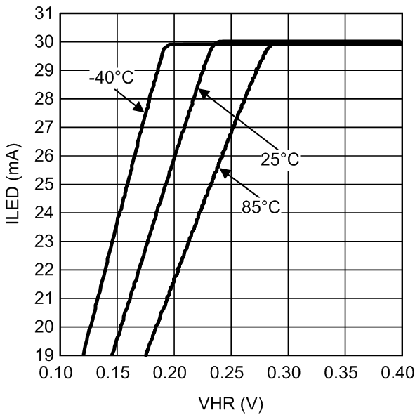
| VHR | Current sink minimum headroom voltage | ILED = 95% of nominal and 20.2 mA | 200 | mV | |||
| ILED = 95% of nominal and 20.2 mA | 240 | ||||||
| RDSON | NMOS switch on resistance | ISW = 100 mA | 0.25 | Ω | |||
| ICL | NMOS switch current limit | 2.7 V ≤ VIN ≤ 5.5 V | 1000 | mA | |||
| 2.7 V ≤ VIN ≤ 5.5 V | 880 | 1000 | 1120 | mA | |||
| VOVP | Output overvoltage protection | ON threshold, 2.7 V ≤ VIN ≤ 5.5 V | 41 | V | |||
| ON threshold, 2.7 V ≤ VIN ≤ 5.5 V | 40 | 42 | |||||
| Hysteresis | 1 | ||||||
| DMAX | Maximum duty cycle | 94% | |||||
| DMIN | Minimum duty cycle | 10% | |||||
| IQ | Quiescent current into IN, device not switching | ILED1 = ILED2 = ILED3 = 20.2 mA, feedback disabled | 490 | µA | |||
| IQ_SW | Switching supply current | ILED1 = ILED2 = ILED3 = 20.2 mA, VOUT = 32 V | 1.35 | mA | |||
| ISHDN | Shutdown current | 2.7 V ≤ VIN ≤ 5.5 V, HWEN = GND | 1 | µA | |||
| 2.7 V ≤ VIN ≤ 5.5 V, HWEN = GND −40°C ≤ TA ≤ +85°C |
2 | ||||||
| ILED_MIN | Minimum LED Current in ILED1, ILED2 or ILED3 | Full-scale current =20.2 mA Brightness code = 0x01, Mapping = Exponential |
9.5 | µA | |||
| TSD | Thermal Shutdown | 140 | °C | ||||
| Hysteresis | 15 | ||||||
| LOGIC INPUTS/OUTPUTS (PWM1, PWM2, HWEN, SCL, SDA, INT) | |||||||
| VIL | Input logic low | 2.7 V ≤ VIN ≤ 5.5 V | 0 | 0.4 | V | ||
| VIH | Input logic high | 2.7 V ≤ VIN ≤ 5.5 V | 1.2 | VIN | |||
| VOL | Output logic low (SCL, INT) | 2.7 V ≤ VIN ≤ 5.5 V, ILOAD = 3 mA | 0.4 | V | |||
| RPWM | PWM input internal pulldown resistance (PWM1, PWM2) | 100 | kΩ | ||||
| AMBIENT LIGHT SENSOR INPUTS (ALS1, ALS2) | |||||||
| RALS1, RALS2 | ALS pin internal pulldown resistors | ALS1, ALS2 Resistor Select Register = 0x0F, 2.7 V ≤ VIN ≤ 5.5 V |
2.44 | kΩ | |||
| ALS1, ALS2 Resistor Select Register = 0x0F, 2.7 V ≤ VIN ≤ 5.5 V |
2.29 | 2.59 | |||||
| VALS_REF | Ambient light sensor reference voltage | 2.7 V ≤ VIN ≤ 5.5 V | 2 | V | |||
| 2.7 V ≤ VIN ≤ 5.5 V | 1.94 | 2.06 | |||||
| VOS | ALS input offset voltage (Code 0-to-1 transition – VLSB) |
2.7 V ≤ VIN ≤ 5.5 V | 2.5 | mV | |||
| 2.7 V ≤ VIN ≤ 5.5 V | 0.8 | 4.2 | |||||
| tCONV | Conversion time | 154 | µs | ||||
| LSB | ADC resolution | 2.7V ≤ VIN ≤ 5.5V | 7.84 | mV | |||
(1) All voltages are with respect to the potential at the GND pin.
(2) Minimum and Maximum limits are verified by design, test, or statistical analysis. Typical numbers are not verified, but do represent the most likely norm.
(3) All current sinks for the matching spec are assigned to the same control bank.
(4) LED current sink matching between ILED2 and ILED3 is given by taking the difference between either (ILED2 or ILED3) and the average current between the two, and dividing by the average current between the two (ILED2/3 – ILED(AVE))/ILED(AVE). This simplifies to (ILED2 – ILED3)/(ILED2 + ILED3). In this test, both ILED2 and ILED3 are assigned to Bank A.
6.6 I2C-Compatible Timing Specifications (SCL, SDA)
See(1)| MIN | NOM | MAX | UNIT | ||
|---|---|---|---|---|---|
| t1 | SCL (clock period) | 2.5 | µs | ||
| t2 | Data In setup time to SCL high | 100 | ns | ||
| t3 | Data out stable after SCL low | 0 | ns | ||
| t4 | SDA low setup time to SCL low (start) | 100 | ns | ||
| t5 | SDA high hold time after SCL high (stop) | 100 | ns | ||
(1) SCL and SDA must be glitch-free in order for proper brightness control to be realized.
6.7 Switching Characteristics
over operating free-air temperature range (unless otherwise noted)| PARAMETER | TEST CONDITIONS | MIN | TYP | MAX | UNIT | |
|---|---|---|---|---|---|---|
| ƒSW | Switching frequency | 2.7 V ≤ VIN ≤ 5.5 V | 500 | kHz | ||
| 2.7 V ≤ VIN ≤ 5.5 V −40°C ≤ TA ≤ 85°C |
450 | 550 | ||||
6.8 Typical Characteristics
VIN = 3.6 V, LEDs (VF = 3.2 V at 20 mA, TA = 25°C), COUT = 1 µF, CIN = 2.2 µF, TA = 25°C unless otherwise specified.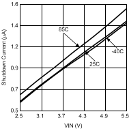
| HWEN = GND |
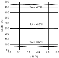
| (ΔILED is worst case difference between all three strings) | ||
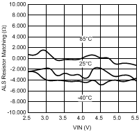
| 2.44-kΩ Setting | ||
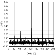


| 2.44-kΩ Setting | ||

