SNVS250F November 2004 – February 2016 LM3670
PRODUCTION DATA.
- 1 Features
- 2 Applications
- 3 Description
- 4 Revision History
- 5 Connection Diagram
- 6 Specifications
- 7 Detailed Description
- 8 Application and Implementation
- 9 Power Supply Recommendations
- 10Layout
- 11Device and Documentation Support
- 12Mechanical, Packaging, and Orderable Information
6 Specifications
6.1 Absolute Maximum Ratings
over operating free-air temperature range (unless otherwise noted)(1)(2)| MIN | MAX | UNIT | ||
|---|---|---|---|---|
| VIN pin: voltage to GND | –0.2 | 6 | V | |
| EN pin: voltage to GND | –0.2 | 6 | V | |
| FB, SW pins | (GND −0.2) | VIN + 0.2 | V | |
| Junction temperature, TJ-MAX | –45 | 125 | °C | |
| Maximum lead temperature (soldering, 10 seconds) | 260 | °C | ||
| Storage temperature, Tstg | –45 | 150 | °C | |
(1) Stresses beyond those listed under Absolute Maximum Ratings may cause permanent damage to the device. These are stress ratings only, which do not imply functional operation of the device at these or any other conditions beyond those indicated under Recommended Operating Conditions. Exposure to absolute-maximum-rated conditions for extended periods may affect device reliability.
(2) If Military/Aerospace specified devices are required, contact the TI Sales Office/Distributors for availability and specifications.
6.2 ESD Ratings
| VALUE | UNIT | |||
|---|---|---|---|---|
| V(ESD) | Electrostatic discharge | Human-body model (HBM), per ANSI/ESDA/JEDEC JS-001(1) | ±2000 | V |
| Charged-device model (CDM), per JEDEC specification JESD22-C101(2) | ±200 | |||
(1) JEDEC document JEP155 states that 500-V HBM allows safe manufacturing with a standard ESD control process.
(2) JEDEC document JEP157 states that 250-V CDM allows safe manufacturing with a standard ESD control process.
6.3 Recommended Operating Conditions
over operating free-air temperature range (unless otherwise noted)(1)| MIN | NOM | MAX | UNIT | ||
|---|---|---|---|---|---|
| Input voltage | 2.5 | 5.5 | A | ||
| Recommended load current | 0 | 350 | mA | ||
| Junction temperature, TJ | –40 | 125 | °C | ||
| Ambient temperature, TA | –40 | 85 | °C | ||
(1) All voltages are with respect to the potential at the GND pin.
6.4 Thermal Information
| THERMAL METRIC(1) | LM3670 | UNIT | |
|---|---|---|---|
| DBV (SOT-23) | |||
| 5 PINS | |||
| RθJA | Junction-to-ambient thermal resistance | 163.3 | °C/W |
| RθJC(top) | Junction-to-case (top) thermal resistance | 114.3 | °C/W |
| RθJB | Junction-to-board thermal resistance | 26.8 | °C/W |
| ψJT | Junction-to-top characterization parameter | 12.4 | °C/W |
| ψJB | Junction-to-board characterization parameter | 26.3 | °C/W |
(1) For more information about traditional and new thermal metrics, see the Semiconductor and IC Package Thermal Metrics application report, SPRA953.
6.5 Electrical Characteristics
Unless otherwise specified, limits for typical values are TJ = 25°C, and minimum and maximum limits apply over the full operating junction temperature range (−40°C ≤ TJ ≤ +125°C); VIN = 3.6 V, VOUT = 1.8 V, IOUT = 150 mA, EN = VIN.| PARAMETER | TEST CONDITIONS | MIN | TYP | MAX | UNIT | |
|---|---|---|---|---|---|---|
| VIN | Input voltage | See(1) | 2.5 | 5.5 | V | |
| VOUT | Fixed output voltage: 1.2 V | 2.5 V ≤ VIN ≤ 5.5 V IOUT = 10 mA |
–2% | 4% | ||
| 2.5 V ≤ VIN ≤ 5.5 V 0 mA ≤ IOUT ≤ 150 mA |
–4.5% | 4% | ||||
| Fixed output voltage: 1.5 V | 2.5 V ≤ VIN ≤ 5.5 V IOUT = 10 mA |
–2.5% | 4% | |||
| 2.5 V ≤ VIN ≤ 5.5 V 0 mA ≤ IOUT ≤ 350 mA |
–5% | 4% | ||||
| Fixed output voltage: 1.6 V, 1.875 V | 2.5 V ≤ VIN ≤ 5.5 V IOUT = 10 mA |
–2.5% | 4% | |||
| 2.5 V ≤ VIN ≤ 5.5V 0 mA ≤ IOUT ≤ 350 mA |
–5.5% | 4% | ||||
| Fixed output voltage: 1.8 V | 2.5 V ≤ VIN ≤ 5.5 V IOUT = 10 mA |
–1.5% | 3% | |||
| 2.5 V ≤ VIN ≤ 5.5 V 0 mA ≤ IOUT ≤ 350 mA |
–4.5% | 3% | ||||
| Fixed output voltage: 3.3 V | 3.6 V ≤ VIN ≤ 5.5 V IOUT = 10 mA |
–2% | 4% | |||
| 3.6V ≤ VIN ≤ 5.5V 0 mA ≤ IOUT ≤ 350 mA |
–6% | 4% | ||||
| Adjustable output voltage(2) | 2.5 V ≤ VIN ≤ 5.5 V IOUT = 10 mA |
–2.5% | 4.5% | |||
| 2.5 V ≤ VIN ≤ 5.5 V 0 mA ≤ IOUT ≤ 150 mA |
–4% | 4.5% | ||||
| Line_reg | Line regulation | 2.5 V ≤ VIN ≤ 5.5 V IOUT = 10 mA |
0.26 | %/V | ||
| Load_reg | Load regulation | 150 mA ≤ IOUT ≤ 350 mA | 0.0014 | %/mA | ||
| VREF | Internal reference voltage | 0.5 | V | |||
| IQ_SHDN | Shutdown supply current | TA = 85ºC | 0.1 | 1 | µA | |
| IQ | DC bias current into VIN | No load, device is not switching (VOUT forced higher than programmed output voltage) | 15 | 30 | µA | |
| VUVLO | Minimum VIN below which VOUT is disabled | TA = −40°C ≤ TJ ≤ 125°C | 2.4 | V | ||
| RDSON (P) | Pin-pin resistance for PFET | VIN = VGS= 3.6V | 360 | 690 | mΩ | |
| RDSON (N) | Pin-pin resistance for NFET | VIN = VGS= 3.6 V | 250 | 660 | mΩ | |
| ILKG (P) | P channel leakage current | VDS = 5.5 V, TA = 25°C | 0.1 | 1 | µA | |
| ILKG (N) | N channel leakage current | VDS = 5.5 V, TA = 25°C | 0.1 | 1.5 | µA | |
| ILIM | Switch peak current limit | 400 | 620 | 750 | mA | |
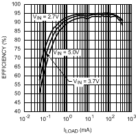
| η | Efficiency | VIN = 3.6 V, VOUT = 1.8 V ILOAD = 1 mA |
91% | |||
| VIN = 3.6 V, VOUT = 1.8 V ILOAD = 10 mA |
94% | |||||
| VIN = 3.6 V, VOUT = 1.8 V ILOAD = 100 mA |
94% | |||||
| VIN = 3.6 V, VOUT = 1.8 V ILOAD = 200 mA |
94% | |||||
| VIN = 3.6 V, VOUT = 1.8 V ILOAD = 300 mA |
92% | |||||
| VIN = 3.6 V, VOUT = 1.8 V ILOAD = 350 mA |
90% | |||||
| VIH | Logic high input | 1.3 | V | |||
| VIL | Logic low input | 0.4 | V | |||
| IEN | Enable (EN) input current | 0.01 | 1 | µA | ||
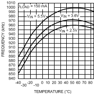
| ƒOSC | Internal oscillator frequency | PWM mode | 550 | 1000 | 1300 | kHz |
(1) The input voltage range recommended for the specified output voltages are given below: VIN = 2.5 V to 5.5 V for 0. 7 V ≤ VOUT < 1.875 V, VIN = ( VOUT + VDROPOUT) to 5.5 for 1.875 ≤ VOUT ≤ 3.3 V, where VDROPOUT = ILOAD × (RDSON (P) + RINDUCTOR).
(2) Output voltage specification for the adjustable version includes tolerance of the external resistor divider.
6.6 Typical Characteristics
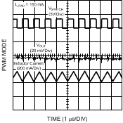
Unless otherwise stated, VIN = 3.6 V and VOUT= 1.8 V.

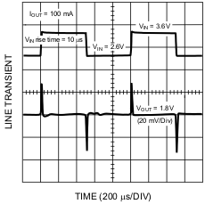
| VIN = 2.6 V to 3.6 V | ILOAD = 100 mA |
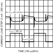
| ILOAD = 3 mA to 280 mA | ||
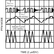

| ILOAD = 350 mA |


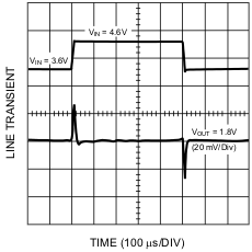
| VIN = 3.6 V to 4.6 V | ILOAD = 100 mA |
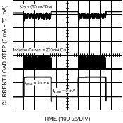
| ILOAD = 0 mA to 70 mA | ||
