JAJSA82S November 2004 – May 2016 LM3671 , LM3671-Q1
PRODUCTION DATA.
- 1 特長
- 2 アプリケーション
- 3 概要
- 4 改訂履歴
- 5 Pin Configuration and Functions
- 6 Specifications
- 7 Detailed Description
- 8 Application and Implementation
- 9 Power Supply Recommendations
- 10Layout
- 11デバイスおよびドキュメントのサポート
- 12メカニカル、パッケージ、および注文情報
パッケージ・オプション
メカニカル・データ(パッケージ|ピン)
サーマルパッド・メカニカル・データ
発注情報
6 Specifications
6.1 Absolute Maximum Ratings
over operating free-air temperature range (unless otherwise noted) (1)(2)| MIN | MAX | UNIT | |
|---|---|---|---|
| VIN pin: voltage to GND | −0.2 | 6 | V |
| FB, SW, EN pins | GND − 0.2 | VIN + 0.2 | V |
| Continuous power dissipation(3) | Internally Limited | ||
| Junction temperature, TJ-MAX | 125 | °C | |
| Maximum lead temperature (soldering, 10 sec.) | 260 | °C | |
| Storage temperature, Tstg | –65 | 150 | °C |
(1) Stresses beyond those listed under Absolute Maximum Ratings may cause permanent damage to the device. These are stress ratings only, which do not imply functional operation of the device at these or any other conditions beyond those indicated under Recommended Operating Conditions. Exposure to absolute-maximum-rated conditions for extended periods may affect device reliability.
(2) If Military/Aerospace specified devices are required, contact the Texas Instruments Sales Office / Distributors for availability and specifications.
(3) Internal thermal shutdown circuitry protects the device from permanent damage. Thermal shutdown engages at TJ= 150°C (typical) and disengages at TJ= 130°C (typical).
6.2 ESD Ratings: LM3671
| VALUE | UNIT | |||
|---|---|---|---|---|
| V(ESD) | Electrostatic discharge | Human-body model (HBM), per ANSI/ESDA/JEDEC JS-001(1) | ±2000 | V |
| Charged-device model (CDM), per JEDEC specification JESD22-C101(2) | ±500 | |||
| Machine model | 200 | |||
(1) JEDEC document JEP155 states that 500-V HBM allows safe manufacturing with a standard ESD control process.
(2) JEDEC document JEP157 states that 250-V CDM allows safe manufacturing with a standard ESD control process.
6.3 ESD Ratings: LM3671-Q1
| VALUE | UNIT | ||||
|---|---|---|---|---|---|
| V(ESD) | Electrostatic discharge | Human-body model (HBM), per AEC Q100-002(1) | ±2000 | V | |
| Charged-device model (CDM), per AEC Q100-011 | All pins except corner pins | ±500 | |||
| Corner pins (1, 3, 4, and 5): SOT-23 | ±750 | ||||
| Corner pins (A1, A3, C1, and C3): DSBGA | ±750 | ||||
| Machine model | ±200 | ||||
(1) AEC Q100-002 indicates that HBM stressing shall be in accordance with the ANSI/ESDA/JEDEC JS-001 specification.
6.4 Recommended Operating Conditions
over operating free-air temperature range (unless otherwise noted)(1)(2)| MIN | MAX | UNIT | |
|---|---|---|---|
| Input voltage(3) | 2.7 | 5.5 | V |
| Recommended load current | 0 | 600 | mA |
| Junction temperature, TJ | –40 | 125 | °C |
| Ambient temperature, TA(4) | –40 | 85 | °C |
(1) Stresses beyond those listed under Absolute Maximum Ratings may cause permanent damage to the device. These are stress ratings only, which do not imply functional operation of the device at these or any other conditions beyond those indicated under Recommended Operating Conditions. Exposure to absolute-maximum-rated conditions for extended periods may affect device reliability.
(2) All voltages are with respect to the potential at the GND pin.
(3) The input voltage range recommended for ideal applications performance for the specified output voltages are given below: VIN = 2.7 V to 4.5 V for 1.1 V ≤ VOUT < 1.5 VIN = 2.7 V to 5.5 V for 1.5 V ≤ VOUT < 1.8 VIN = (VOUT + VDROPOUT) to 5.5 V for 1.8 V ≤ VOUT ≤ 3.3 V where VDROPOUT = ILOAD × (RDSON, PFET + RINDUCTOR).
(4) In applications where high power dissipation and/or poor package resistance is present, the maximum ambient temperature may have to be derated. Maximum ambient temperature (TA-MAX) is dependent on the maximum operating junction temperature (TJ-MAX), the maximum power dissipation of the device in the application (PD-MAX) and the junction to ambient thermal resistance of the package (RθJA) in the application, as given by the following equation: TA-MAX = TJ-MAX − (RθJA × PD-MAX). Refer to Dissipation Ratings for PD-MAX values at different ambient temperatures.
6.5 Thermal Information
| THERMAL METRIC(1) | LM3671 | LM3671 and LM3671-Q1 | UNIT | ||
|---|---|---|---|---|---|
| NKH (USON) | DBV (SOT-23 ) | YZR (DSBGA) | |||
| 6 PINS | 5 PINS | 5 PINS | |||
| RθJA | Junction-to-ambient thermal resistance | 174.7 | 165.7 | 181.0 | °C/W |
| RθJC(top) | Junction-to-case (top) thermal resistance | 87.1 | 116.6 | 0.9 | °C/W |
| RθJB | Junction-to-board thermal resistance | 109.0 | 26.8 | 110.3 | °C/W |
| ψJT | Junction-to-top characterization parameter | 6.4 | 13.3 | 7.4 | °C/W |
| ψJB | Junction-to-board characterization parameter | 109.0 | 26.3 | 110.3 | °C/W |
(1) For more information about traditional and new thermal metrics, see the Semiconductor and IC Package Thermal Metrics application report, SPRA953.
6.6 Dissipation Ratings
6.7 Electrical Characteristics
Unless otherwise noted, limits apply for for TJ = 25°C, and specifications apply to the LM3671MF/TL/LC with VIN = EN = 3.6 V(1)(2)(3)| PARAMETER | TEST CONDITION | MIN | TYP | MAX | UNIT | |
|---|---|---|---|---|---|---|
| VIN | Input voltage | −40°C to 125°C, see(3) | 2.7 | 5.5 | V | |
| VFB | Feedback voltage (fixed) MF | PWM mode(4), −40°C to 125°C | −4% | 4% | ||
| Feedback voltage (fixed) TL | −2.5% | 2.5% | ||||
| Feedback voltage (fixed) LC | −4% | 4% | ||||
| Feedback voltage (ADJ) MF(5) | PWM mode(4), −40°C to 125°C | −4% | 4% | |||
| Feedback voltage (ADJ) TL | −2.5 | 2.5 | ||||
| Line regulation | 2.7 V ≤ VIN ≤ 5.5 V, IO = 10 mA | 0.031 | %/V | |||
| Load regulation | 100 mA ≤ IO ≤ 600 mA, VIN = 3.6 V | 0.0013 | %/mA | |||
| VREF | Internal reference voltage | 0.5 | V | |||
| ISHDN | Shutdown supply current | EN = 0 V | 0.01 | µA | ||
| EN = 0 V, −40°C to 125°C | 1 | |||||
| IQ | DC bias current into VIN | No load, device is not switching (FB forced higher than programmed output voltage) | 16 | µA | ||
| No load, device is not switching (FB forced higher than programmed output voltage), −40°C to 125°C | 35 | |||||
| RDSON (P) | Pin-pin resistance for PFET | VIN = VGS = 3.6 V | 380 | 500 | mΩ | |
| RDSON (N) | Pin-pin resistance for NFET | VIN = VGS= 3.6 V | 250 | 400 | mΩ | |
| ILIM | Switch peak current limit | Open loop(6) | 1020 | mA | ||
| Open loop(6), −40°C to 125°C | 830 | 1150 | ||||
| VIH | Logic high input | −40°C to 125°C | 1 | V | ||
| VIL | Logic low input | −40°C to 125°C | 0.4 | V | ||
| IEN | Enable (EN) input current | 0.01 | µA | |||
| −40°C to 125°C | 1 | |||||
| ƒOSC | Internal oscillator frequency | PWM Mode(4) | 2 | MHz | ||
| PWM Mode(4), −40°C to 125°C | 1.6 | 2.6 | ||||
(1) Minimum (MIN) and maximum (MAX) limits are specified by design, test or statistical analysis. Typical (TYP) numbers are not specified, but do represent the most likely norm.
(2) The parameters in the electrical characteristic table are tested at VIN = 3.6 V unless otherwise specified. For performance over the input voltage range refer to datasheet curves.
(3) The input voltage range recommended for ideal applications performance for the specified output voltages are given below: VIN = 2.7 V to 4.5 V for 1.1 V ≤ VOUT < 1.5 VIN = 2.7 V to 5.5 V for 1.5 V ≤ VOUT < 1.8 VIN = (VOUT + VDROPOUT) to 5.5 V for 1.8 V ≤ VOUT ≤ 3.3 V where VDROPOUT = ILOAD × (RDSON, PFET + RINDUCTOR).
(4) Test condition: for VOUT less than 2.5 V, VIN = 3.6 V; for VOUT greater than or equal to 2.5 V, VIN = VOUT + 1 V.
(5) ADJ version is configured to 1.5 V output. For ADJ output version: VIN = 2.7 V to 4.5 V for 0.9 V ≤ VOUT < 1.1 VIN = 2.7 V to 5.5 V for 1.1 V ≤ VOUT < 3.3 V
(6) Refer to Typical Characteristics for closed-loop data and its variation with regards to supply voltage and temperature. Electrical Characteristics reflects open-loop data (FB = 0 V and current drawn from SW pin ramped up until cycle by cycle current limit is activated). Closed loop current limit is the peak inductor current measured in the application circuit by increasing output current until output voltage drops by 10%.
6.8 Typical Characteristics
LM3671MF/TL/LC, circuit of Figure 32, VIN = 3.6 V, VOUT = 1.5 V, TA = 25°C, unless otherwise noted.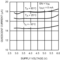 Figure 1. Quiescent Supply Current vs Supply Voltage
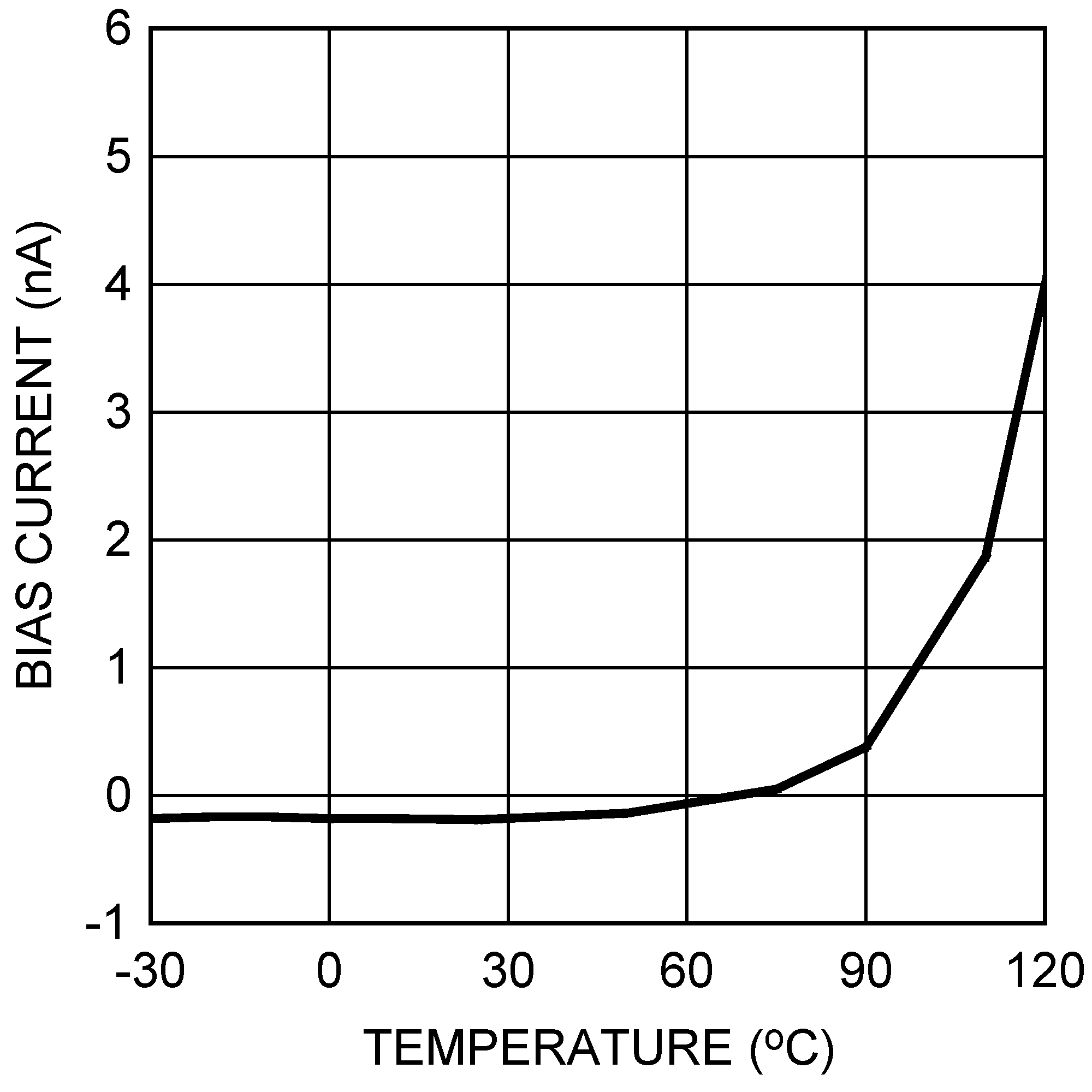 Figure 3. Feedback Bias Current vs Temperature
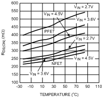 Figure 5. RDS(ON) vs. Temperature
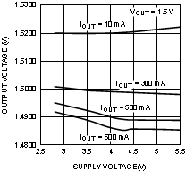
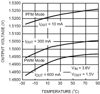
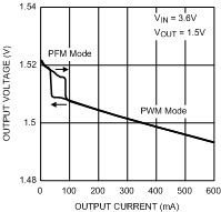
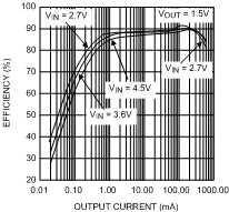
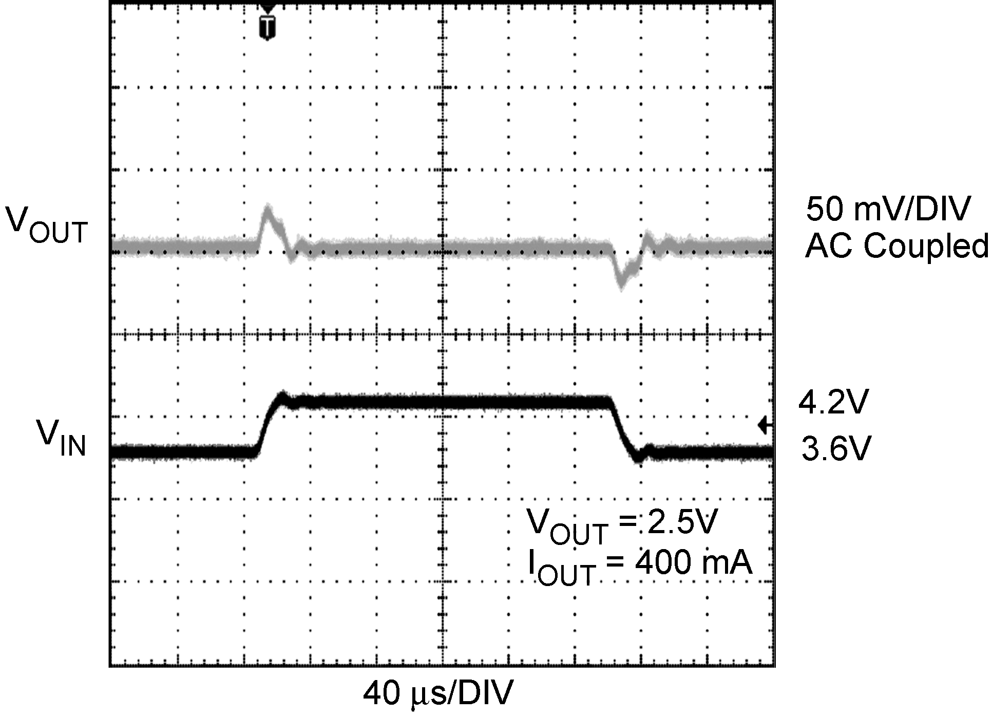
| L = 2.2 µH |
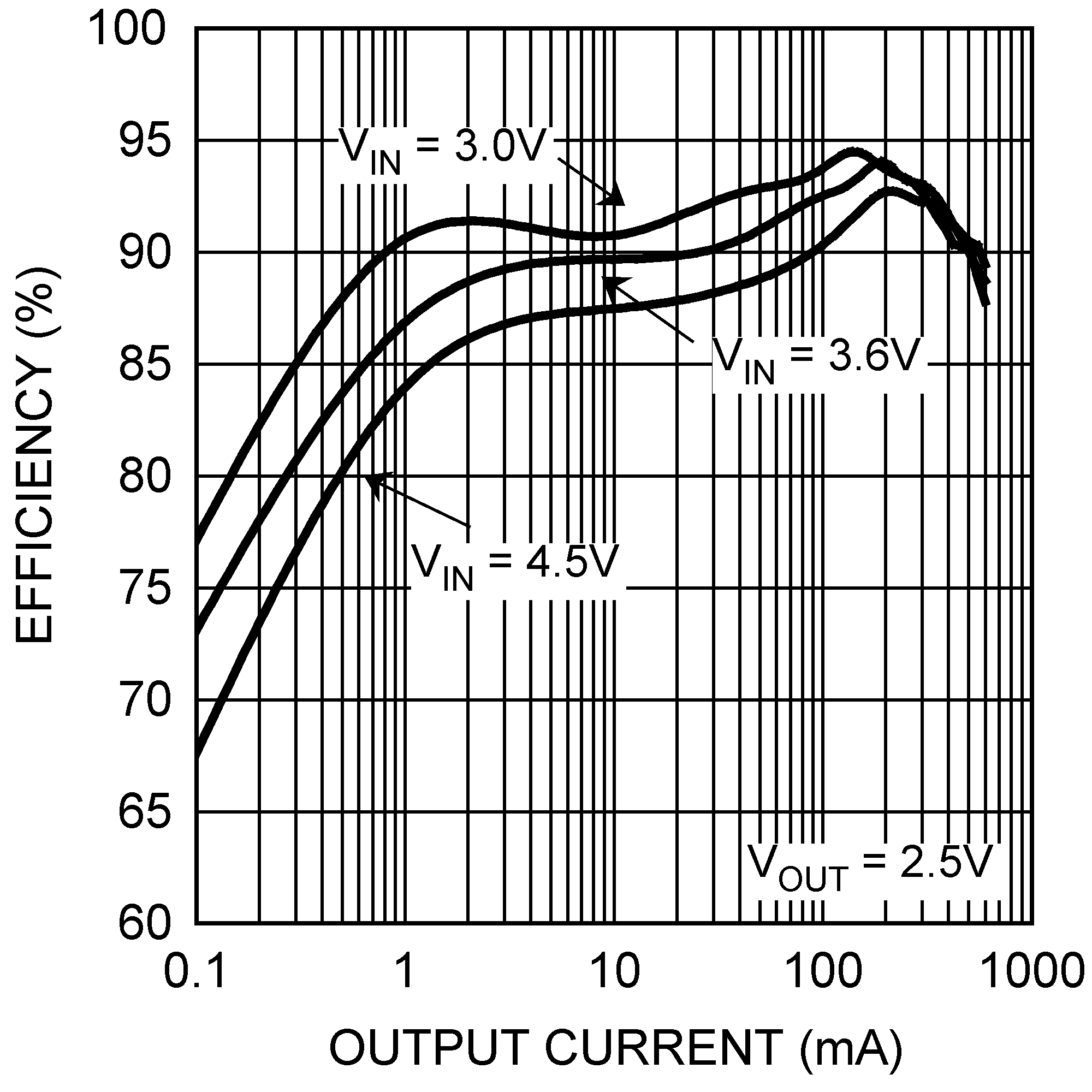
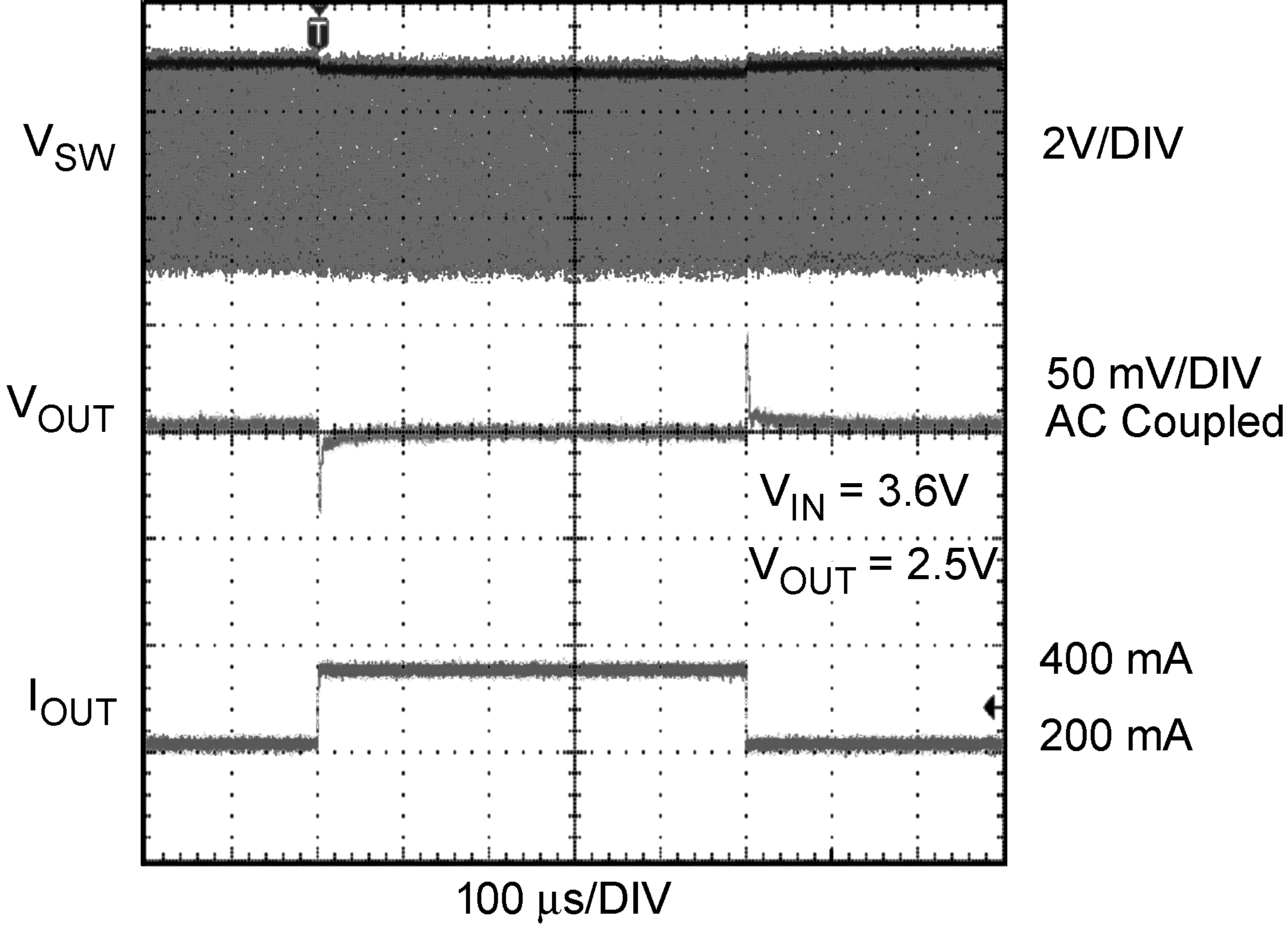
| L = 2.2 µH | ||
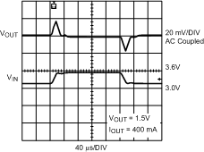
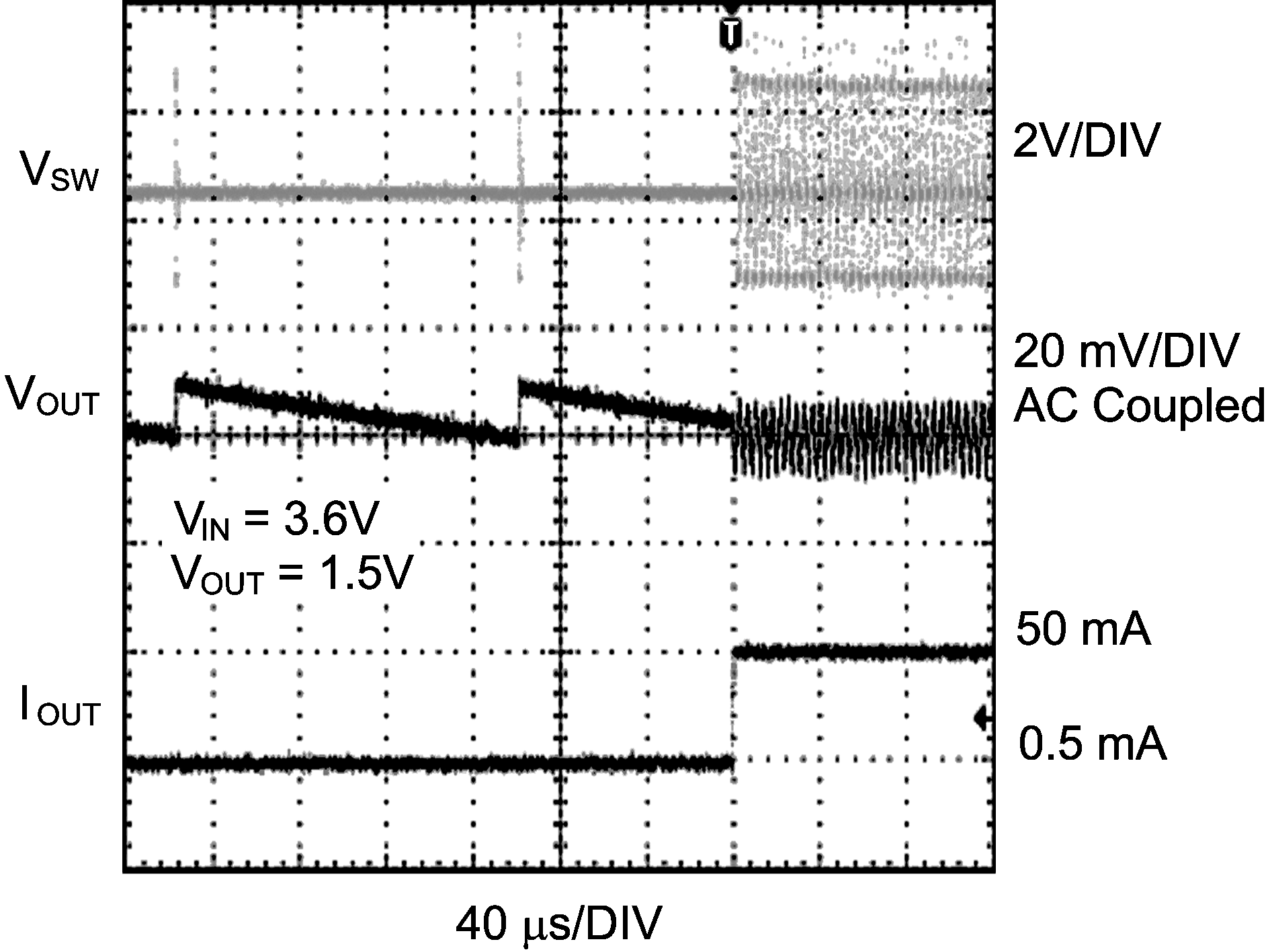
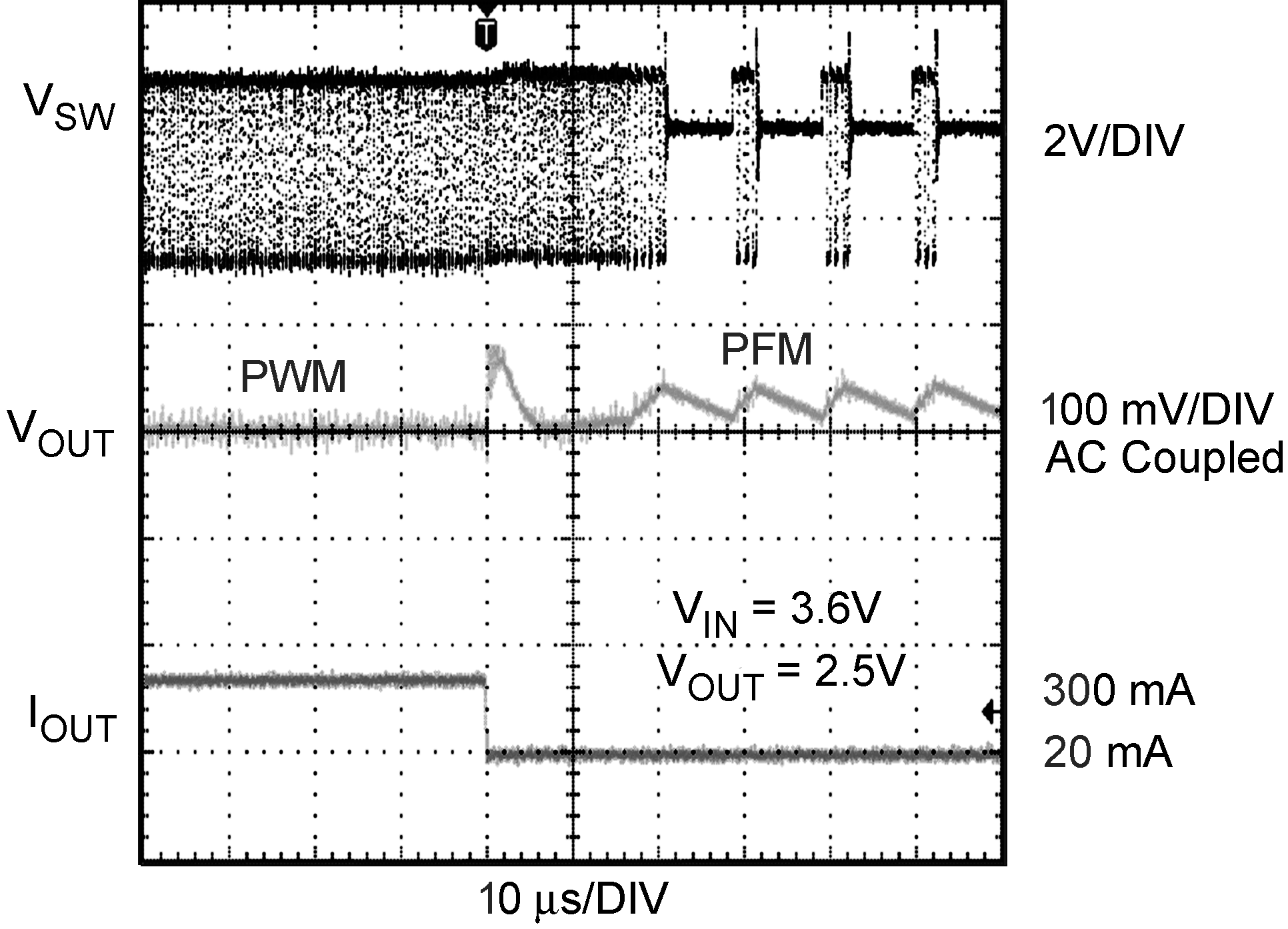
| PFM Mode 0.5 mA to 50 mA | ||
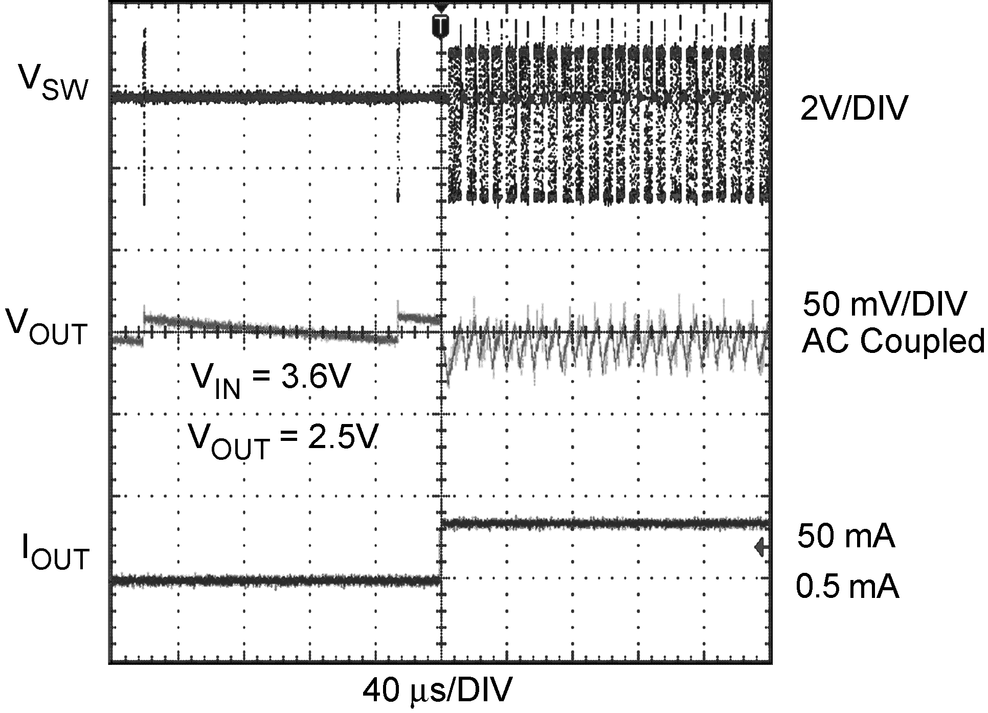
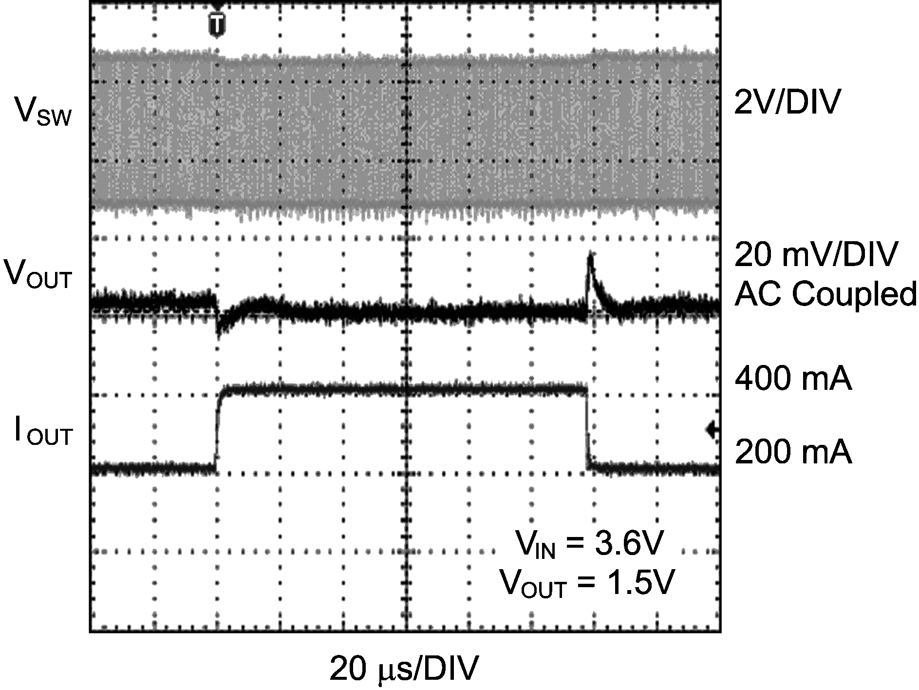
| PFM Mode 0.5 mA to 50 mA | ||
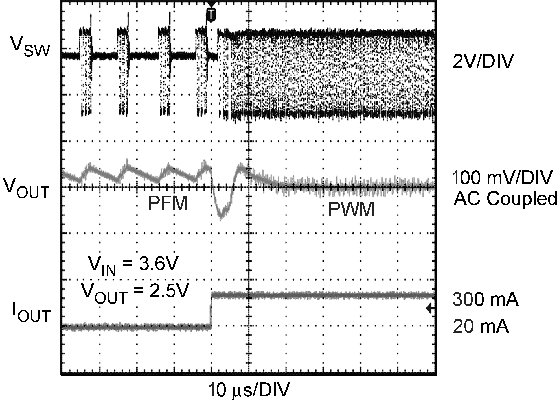
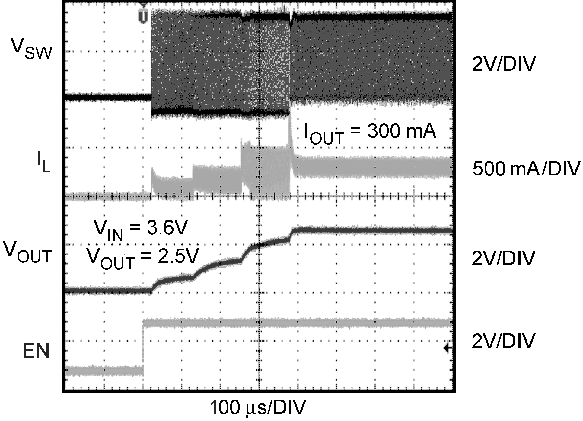
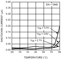 Figure 2. Shutdown Current vs Temp
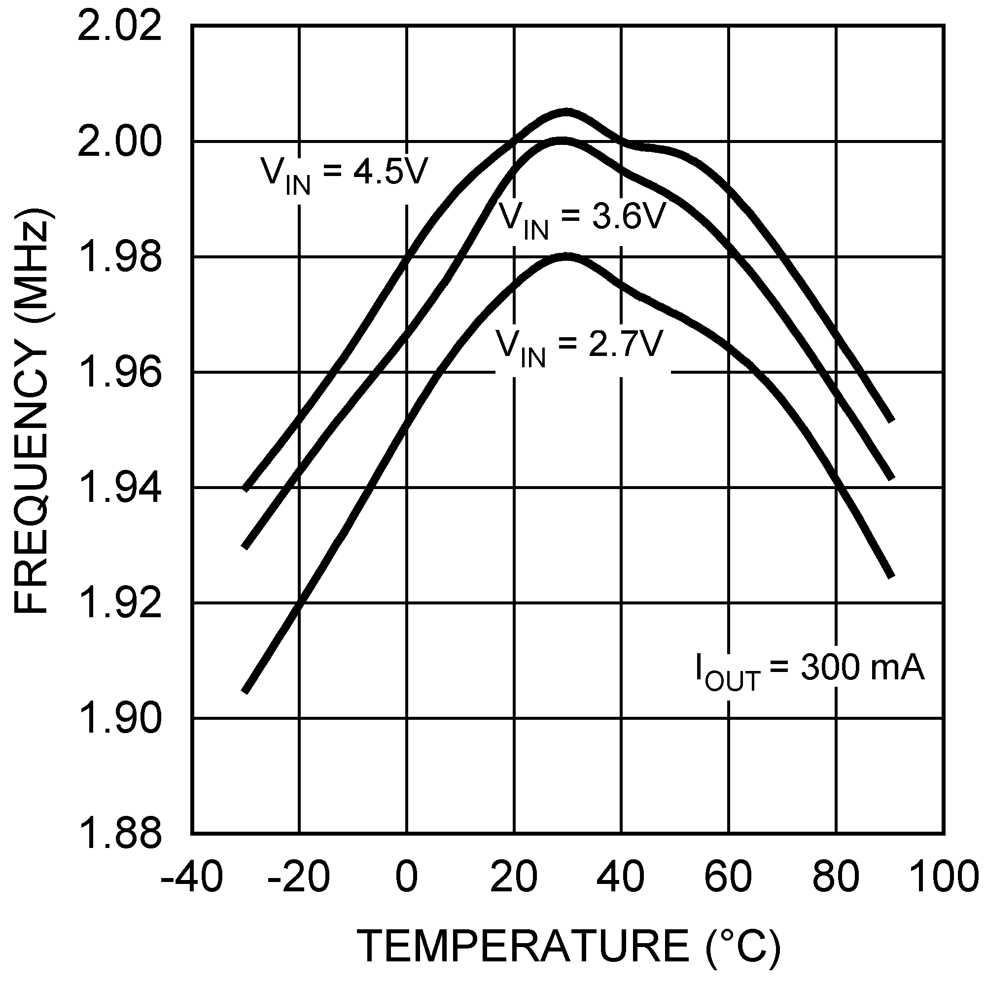 Figure 4. Switching Frequency vs Temperature
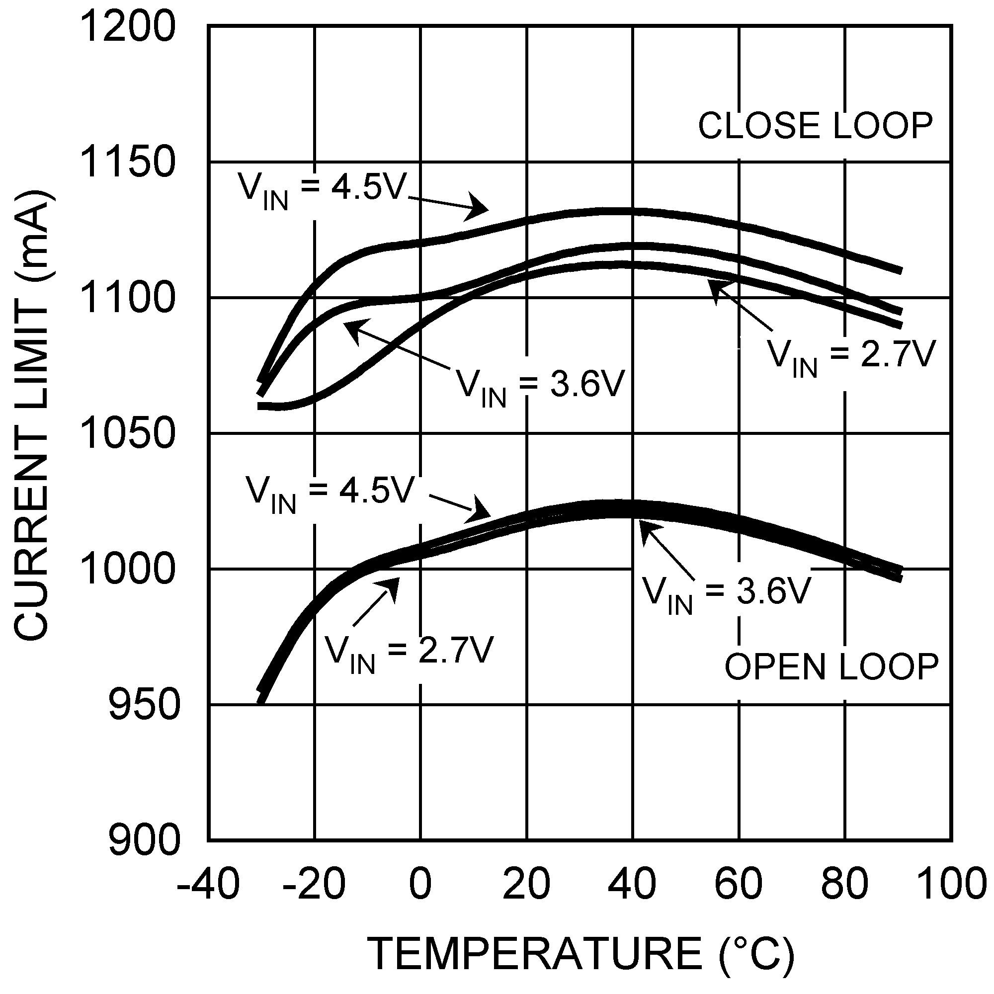 Figure 6. Open/Closed Loop Current Limit vs Temperature
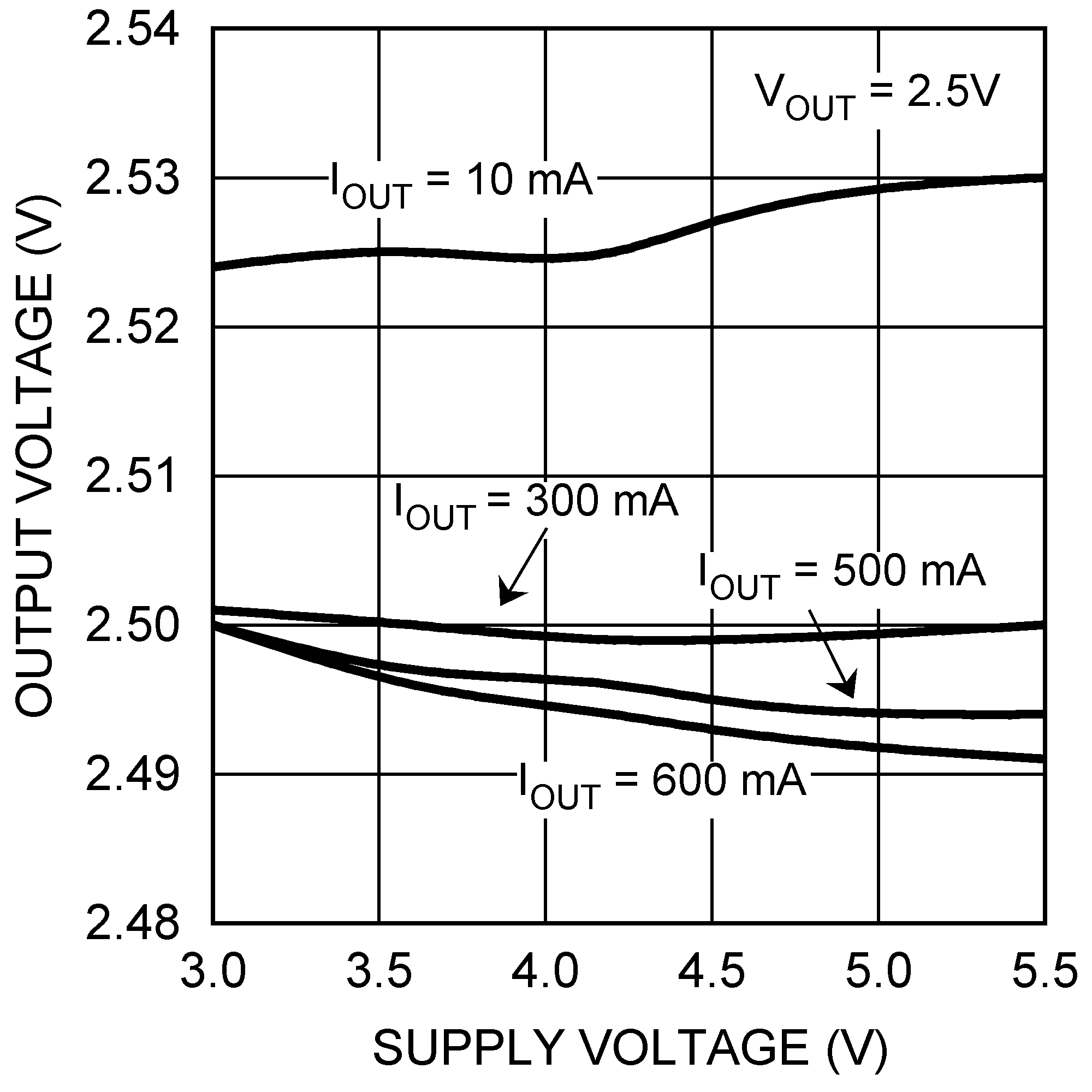
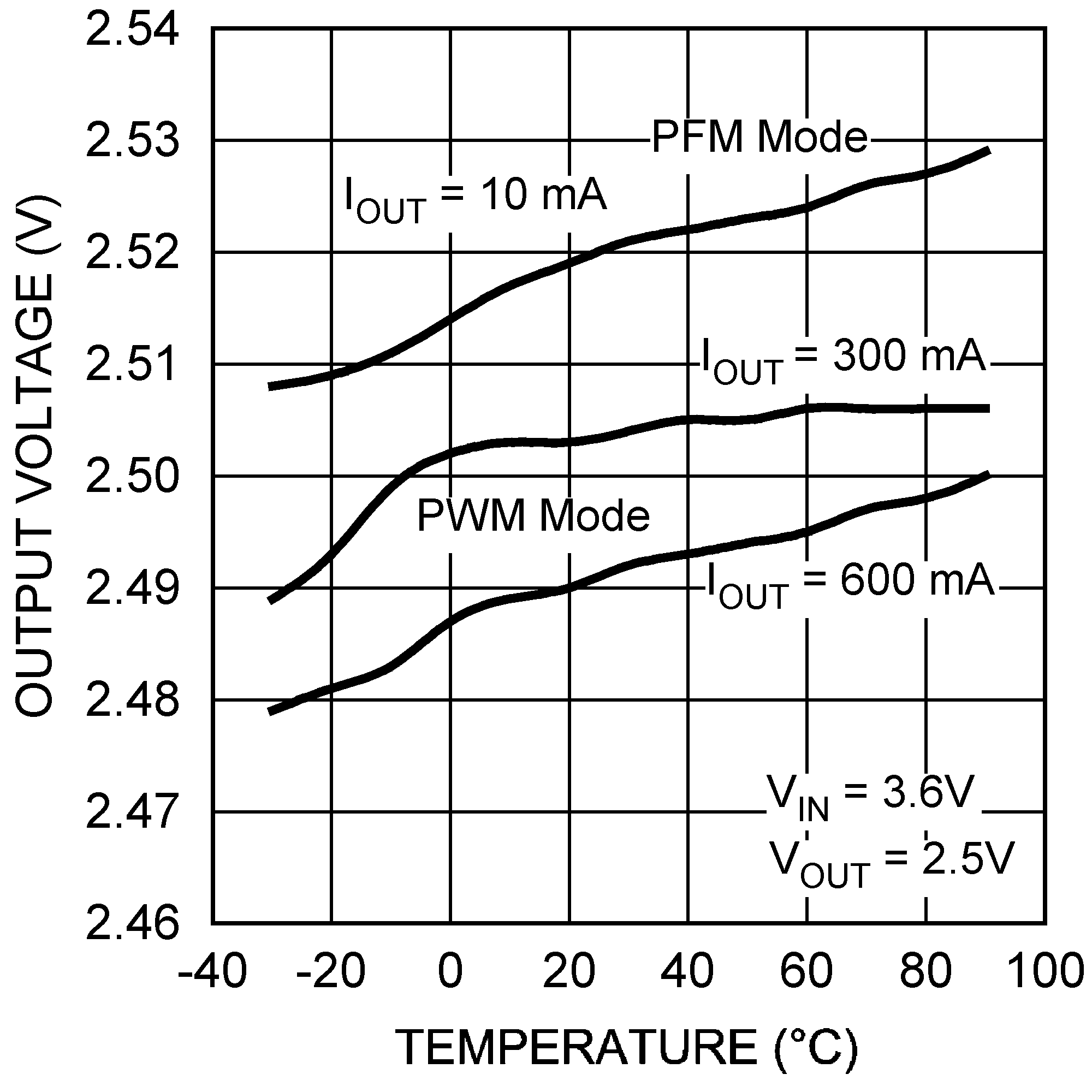
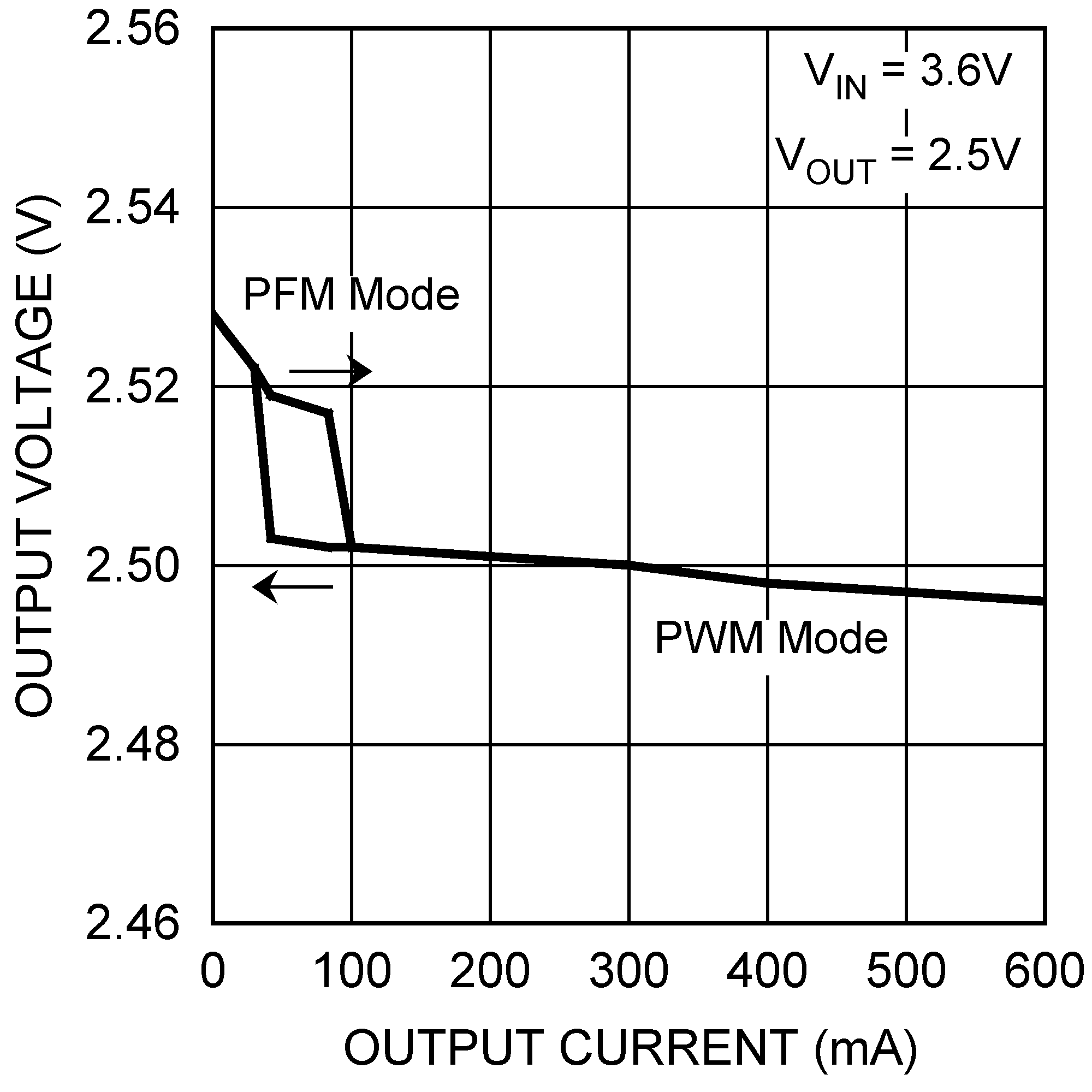
| L = 2.2 µH |
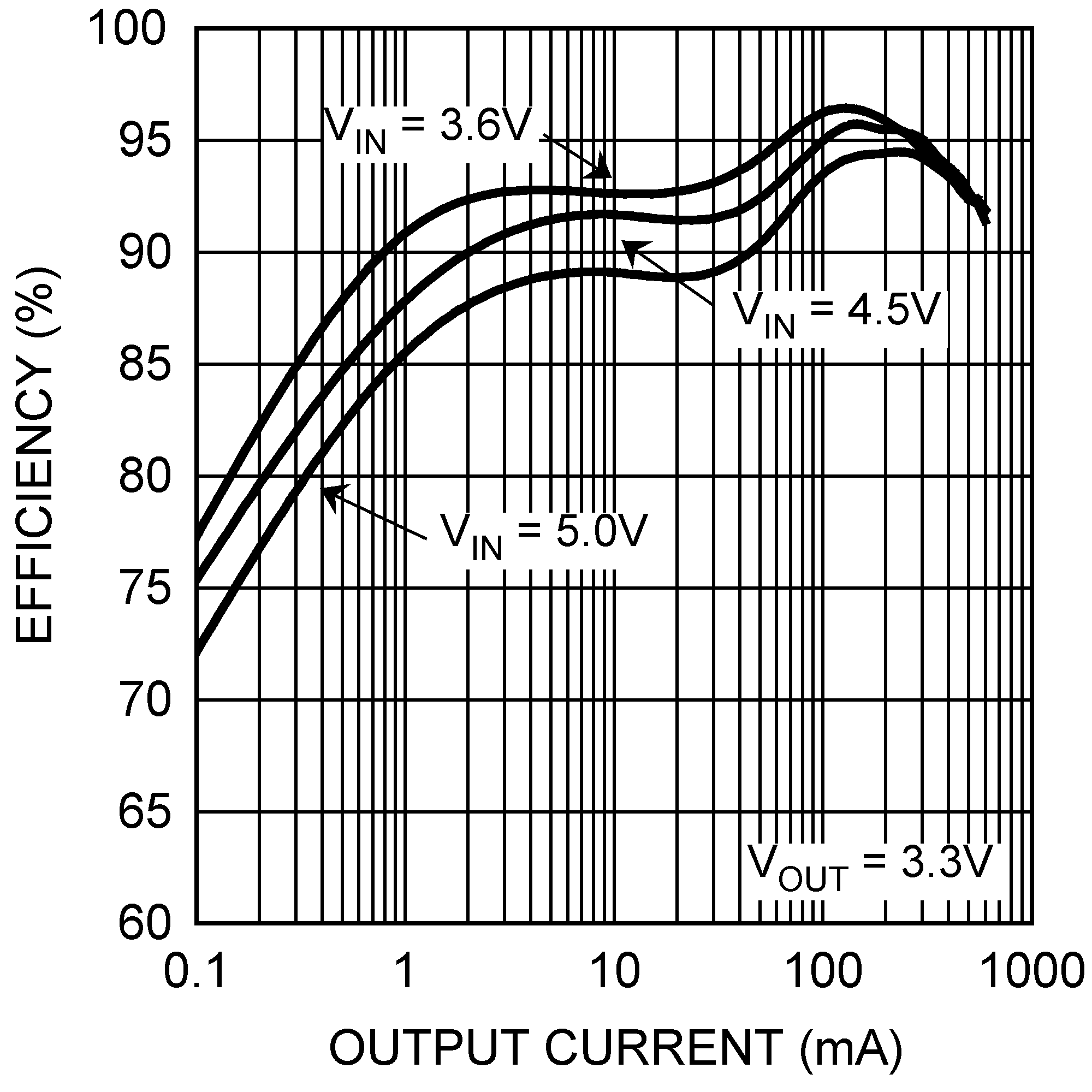
| L = 2.2 µH | ||
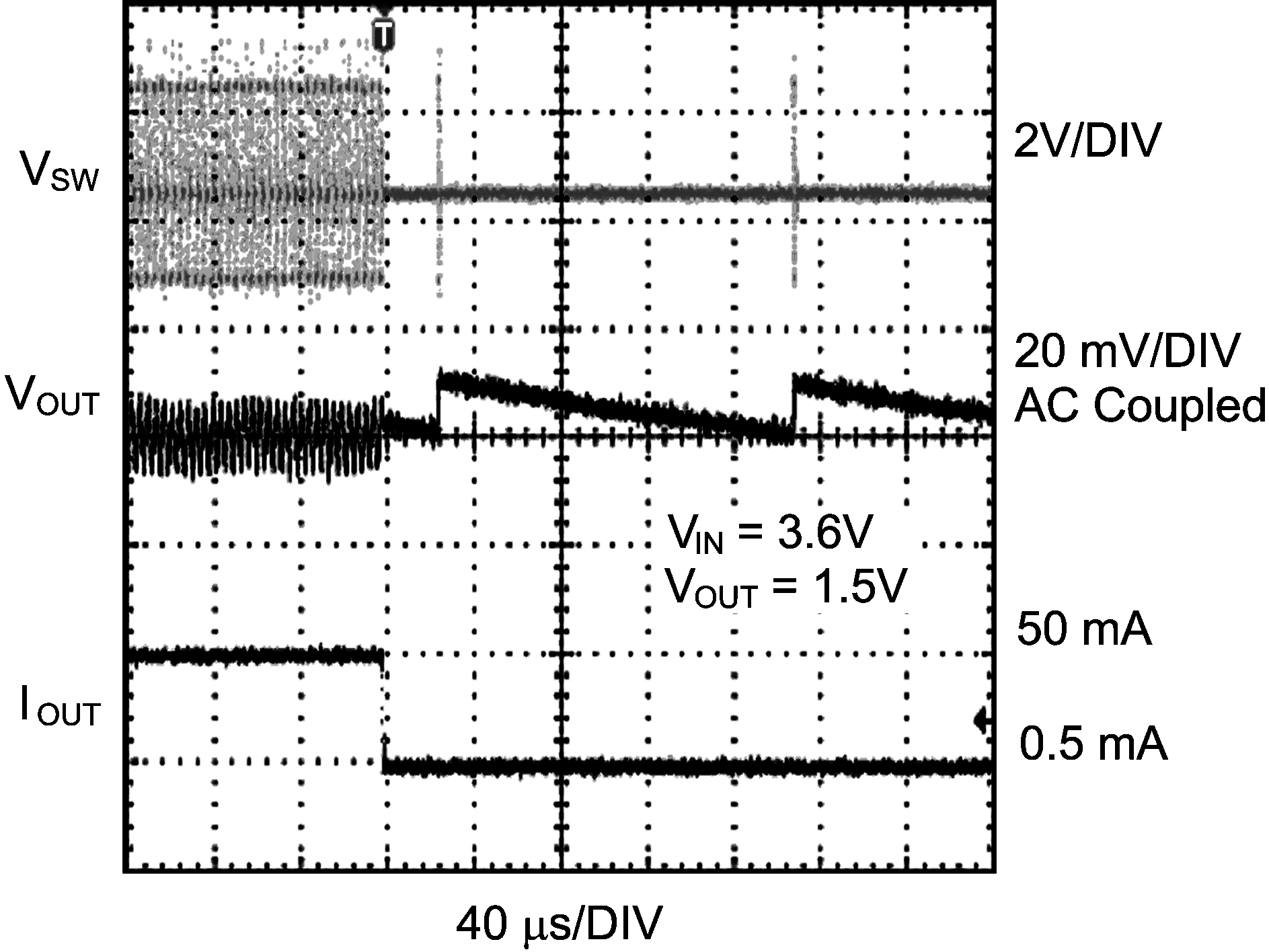
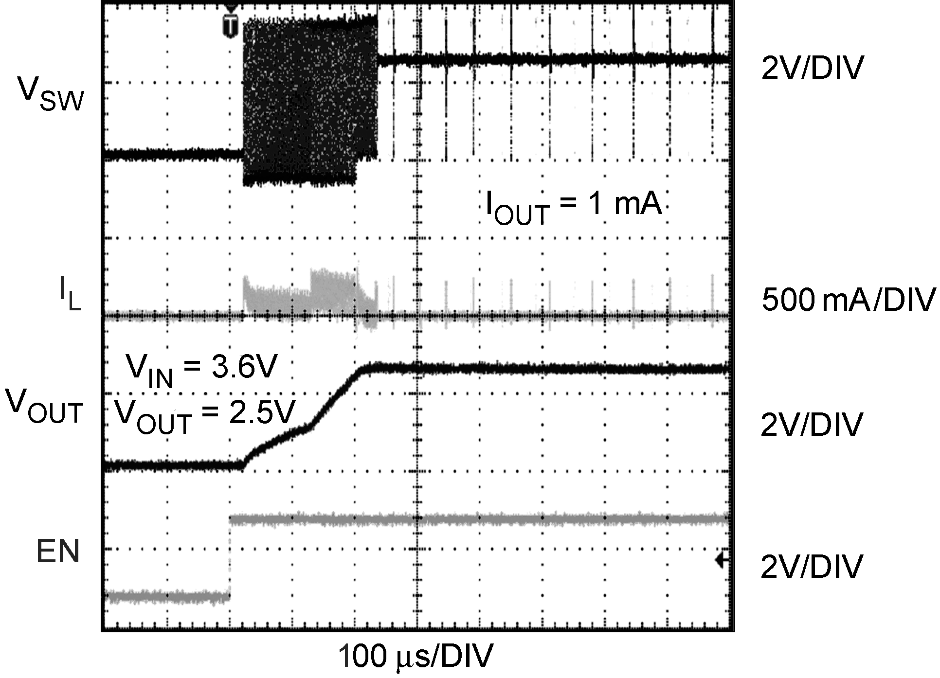
| PFM Mode 0.5 mA to 50 mA | ||
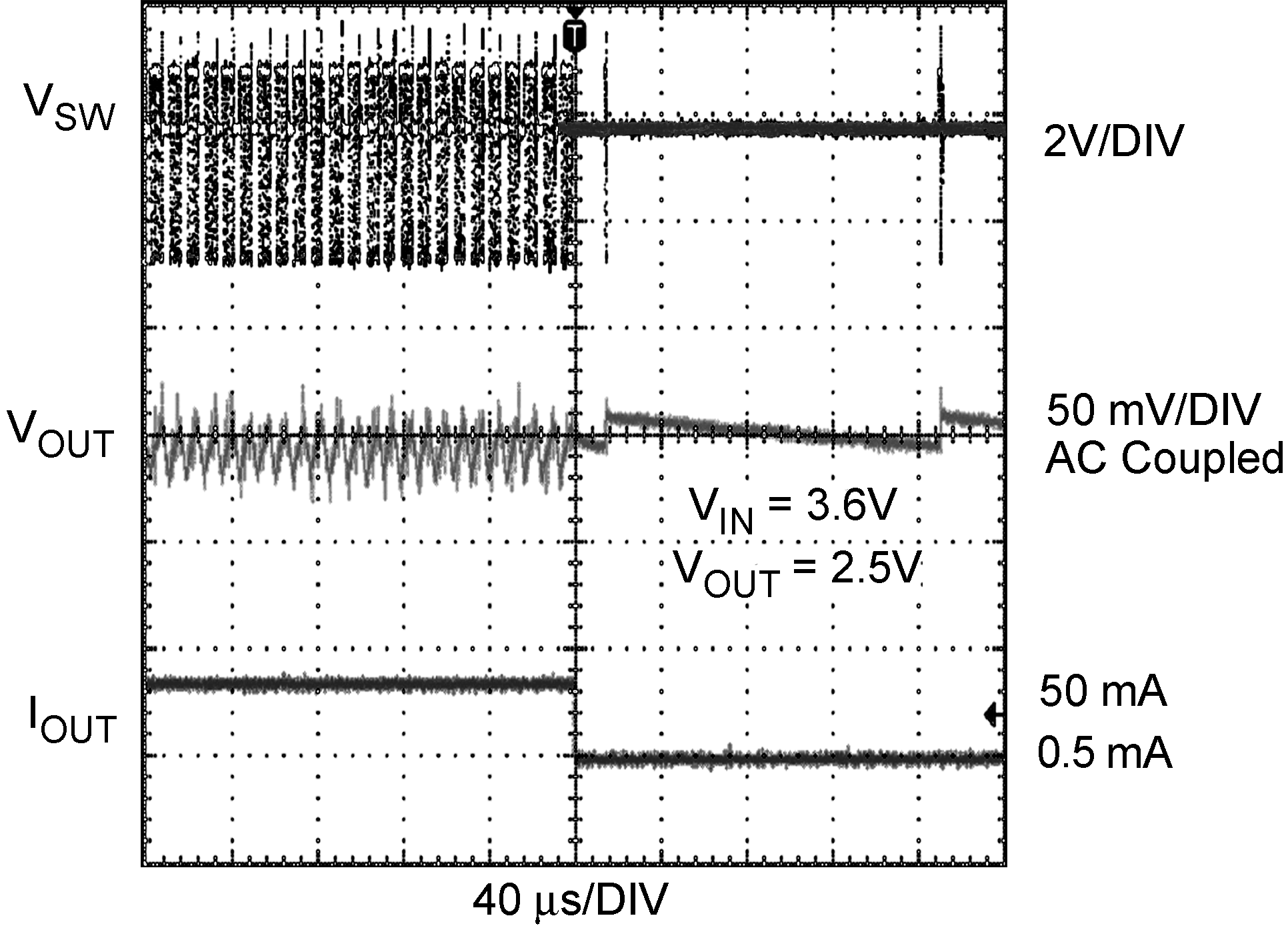
| PFM Mode 50 mA to 0.5 mA | ||
