SNVS520F August 2008 – November 2016 LM3686
PRODUCTION DATA.
- 1 Features
- 2 Applications
- 3 Description
- 4 Revision History
- 5 Description (Continued)
- 6 Pin Configuration and Functions
-
7 Specifications
- 7.1 Absolute Maximum Ratings
- 7.2 ESD Ratings
- 7.3 Recommended Operating Conditions
- 7.4 Thermal Information
- 7.5 Electrical Characteristics: Linear Regulator - LILO
- 7.6 Electrical Characteristics: Linear Regulator - LDO
- 7.7 Electrical Characteristics: DC-DC Converter
- 7.8 Electrical Characteristics: Global Parameters (DCDC, LILO, and LDO)
- 7.9 Typical Characteristics
- 8 Detailed Description
- 9 Application and Implementation
- 10Power Supply Recommendations
- 11Layout
- 12Device and Documentation Support
- 13Mechanical, Packaging, and Orderable Information
9 Application and Implementation
NOTE
Information in the following applications sections is not part of the TI component specification, and TI does not warrant its accuracy or completeness. TI’s customers are responsible for determining suitability of components for their purposes. Customers should validate and test their design implementation to confirm system functionality.
9.1 Application Information
The LM3686 is a step-down DC-DC converter with integrated low-dropout linear regular and a low-noise linear regulator optimized for powering ultra-low voltage circuits from a single Li-Ion cell or 3-cell NiMH/NiCd batteries. It provides three outputs with combined load current up to 900 mA over an input-voltage range from 2.7 V to 5.5 V.
9.2 Typical Application
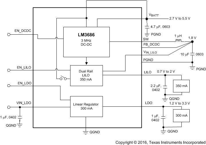 Figure 16. LM3686 Typical Application
9.2.1 Design Requirements
For typical step-down DC-DC converter applications, use the parameters listed in Table 2.
Table 2. Design Parameters
| DESIGN PARAMETER | EXAMPLE VALUE |
|---|---|
| Input voltage | 2.7 V to 5.5 V |
| Output voltage | 1.8 V |
| Output current | 100 mA |
| Minimum switching frequency | 2.55 MHz |
| RMS noise, 10 Hz to100 kHz | 166 μVRMS |
| PSRR at 100 kHz | 60 dB |
9.2.2 Detailed Design Procedure
9.2.2.1 Application Selection
TI strongly recommends selection of the required components for the LM3686 device as described within the data sheet. If other components are selected, the device will not perform up to standards, and electrical characteristics cannot be ensured.
9.2.2.2 Inductor Selection
There are two main considerations when choosing an inductor: the inductor must not saturate, and the inductor current ripple must be small enough to achieve the desired output voltage ripple. Different saturation current rating specifications are followed by different manufacturers so attention must be given to details. Saturation current ratings are typically specified at 25°C. However, ratings at the maximum ambient temperature of application should be requested from the manufacturer. The minimum value of inductance to ensure good performance is 0.7 µH at ILIM (typical) DC current over the ambient temperature range. Shielded inductors radiate less noise and are preferred. There are two methods to choose the inductor saturation current rating.
9.2.2.2.1 Method 1
The saturation current must be greater than the sum of the maximum load current and the worst case average-to-peak inductor current. This can be written as:
where

where
- IRIPPLE: average-to-peak inductor current
- IOUT_DCDCMAX: maximum load current (600 mA)
- VBATT: maximum input voltage in application
- L: minimum inductor value including worst case tolerances (30% drop can be considered for Method 1)
- f: minimum switching frequency (2.55 MHz)
9.2.2.2.2 Method 2
A more conservative and recommended approach is to choose an inductor that has a saturation current rating greater than the maximum current limit of 1375 mA.
A 1-µH inductor with a saturation current rating of at least 1375 mA is recommended for most applications. Resistance of the inductor must less than 0.3 Ω for good efficiency. Table 3 lists suggested inductors and suppliers. For low-cost applications, an unshielded bobbin inductor could be considered. For noise critical applications, a toroidal or shielded- bobbin inductor should be used. A good practice is to lay out the board with overlapping footprints of both types for design flexibility. This allows substitution of a low-noise shielded inductor, in the event that noise from low-cost bobbin models is unacceptable.
Table 3. Suggested Inductors and Their Suppliers
| MODEL | VENDOR | DIMENSIONS L × W × H (mm) | DCR (maximum) |
|---|---|---|---|
| BRL2518T1R0M | TAIYO YUDEN | 2.5 × 1.8 × 1.2 | 80 |
| MDT2520CR1R0M | TOKO | 2.5 × 2.0 × 1.0 | 80 |
| KSLI252010AG1R0 | HITACHI METALS | 2.5 × 2.0 × 1.0 | 75 |
9.2.2.3 External Capacitors
As common with most regulators, the LM3686 requires external capacitors to ensure stable operation. The LM3686 is specifically designed for portable applications requiring minimum board space and the smallest size components. These capacitors must be correctly selected for good performance.
9.2.2.4 Input Capacitor Selection
9.2.2.4.1 CIN_DC-DC
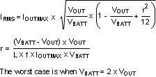
A ceramic input capacitor of 4.7 µF, 6.3 V is sufficient for most applications. Place the input capacitor as close as possible to the VBATT pin of the device. A larger value may be used for improved input voltage filtering. Use X7R or X5R types; do not use Y5V. DC bias characteristics of ceramic capacitors must be considered when selecting case sizes like 0805 and 0603. The minimum input capacitance to ensure good performance is 2.2 µF at 3-V DC bias; 1.5 µF at 5-V DC bias including tolerances and over ambient temperature range. The input filter capacitor supplies current to the PFET switch of the LM3686 DC-DC converter in the first half of each cycle and reduces voltage ripple imposed on the input power source. The low ESR of a ceramic capacitor provides the best noise filtering of the input voltage spikes due to this rapidly changing current. Select a capacitor with sufficient ripple current rating. The input current ripple can be calculated as:
9.2.2.4.2 CIN_LILO
If the LILO is used as post regulation no additional capacitor is needed at VIN_LILO as the output filter capacitor of the DC-DC converter is close by and therefore sufficient.
In case of independent mode use, a 1-µF ceramic capacitor is recommended at VIN_LILO if no other filter capacitor is present in the VIN_LILO supply path. This capacitor must be located a distance of not more than 1 cm from the VIN_LILO input pin and returned to QGND.
9.2.2.4.3 CIN_LDO
An input capacitor is required for stability. TI recommends using a 1-µF ceramic capacitor and connected between the VIN_LDO and QGND.
9.2.2.5 Output Capacitor
9.2.2.5.1 COUT_DCDC
A ceramic output capacitor of 10 µF, 6.3 V is sufficient for most applications. Use X7R or X5R types; do not use Y5V. DC bias characteristics of ceramic capacitors must be considered when selecting case sizes like 0805 and 0603. DC bias characteristics vary from manufacturer to manufacturer, and DC bias curves should be requested from them as part of the capacitor selection process.
The minimum output capacitance to ensure good performance is 5.75 µF at 1.8-V DC bias including tolerances and over ambient temperature range. The output filter capacitor smooths out current flow from the inductor to the load, helps maintain a steady output voltage during transient load changes and reduces output voltage ripple. These capacitors must be selected with sufficient capacitance and sufficiently low equivalent series resistance (ESR) to perform these functions.
The output voltage ripple is caused by the charging and discharging of the output capacitor and by the RESR and can be calculated as:
Voltage peak-to-peak ripple due to capacitance can be expressed as:

Voltage peak-to-peak ripple due to ESR can be expressed as:
Because these two components are out of phase, the root mean squared (RMS) value can be used to get an approximate value of peak-to-peak ripple. The peak-to-peak ripple voltage, RMS value can be expressed as:

Note that the output voltage ripple is dependent on the inductor current ripple and the ESR of the output capacitor (RESR). The RESR is frequency dependent (as well as temperature dependent); make sure the value used for calculations is at the switching frequency of the part.
9.2.2.5.2 COUT_LILO
The linear regulator is designed specifically to work with very small ceramic output capacitors. A ceramic capacitor (dielectric types X7R, Z5U, or Y5V) in the 2.2-µF range (up to 10 µF) and with an ESR between 3 mΩ to 300 mΩ is suitable as COUT_LIN in the LM3686 application circuit.
This capacitor must be located a distance of not more than 1 cm from the VOUT_LILO pin and returned to a clean analog ground. Tantalum or film capacitors may also be used at the device output, VOUT_LILO but these are not as attractive for reasons of size and cost (see Table 4).
9.2.2.5.3 COUT_LDO
A ceramic capacitor in the 1-uF to 2.2-uF range, and with ESR between 5 mΩ to 500 mΩ, is suitable for the linear regulator. Connect this output capacitor no more than 1 cm from VOUT_LDO and QGND.
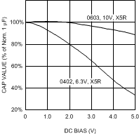 Figure 17. Graph Showing A Typical Variation In Capacitance vs DC Bias
Table 4. Suggested Capacitors and Their Suppliers
| CAPACITANCE (µF) | MODEL | VOLTAGE RATING (V) | Vendor | Type | Case Size / Inch (mm) |
|---|---|---|---|---|---|
| 10 | C1608X5R0J106K | 6.3 | TDK | Ceramic, X5R | 0603 (1608) |
| 4.7 | C1608X5R0J475 | 6.3 | TDK | Ceramic, X5R | 0603 (1608) |
| 2.2 | C1608X5R0J225M | 6.3 | TDK | Ceramic, X5R | 0603 (1608) |
| 1 | C1005JB0J105KT | 6.3 | TDK | Ceramic, X5R | 0402 (1005) |
9.2.3 Application Curves
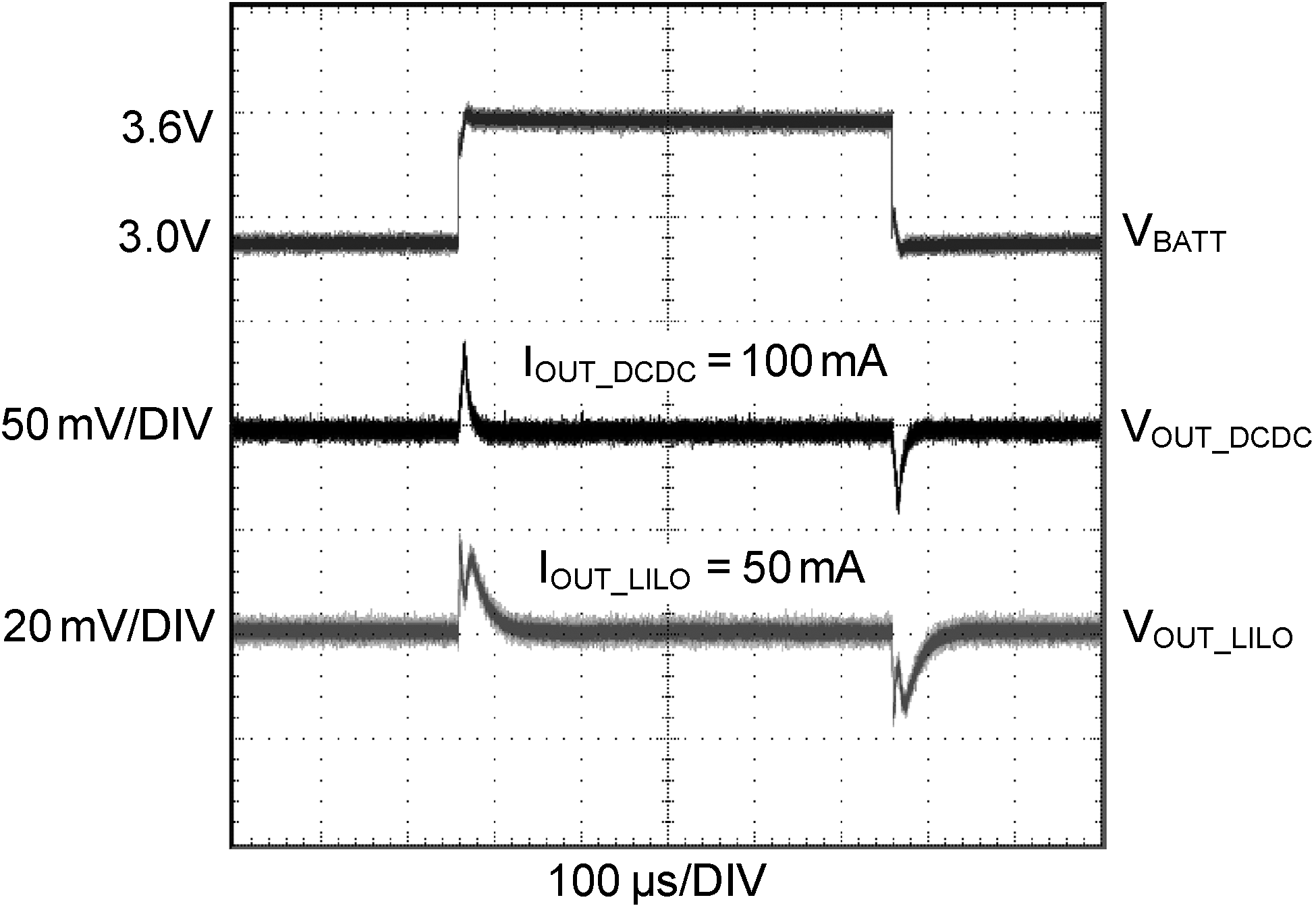
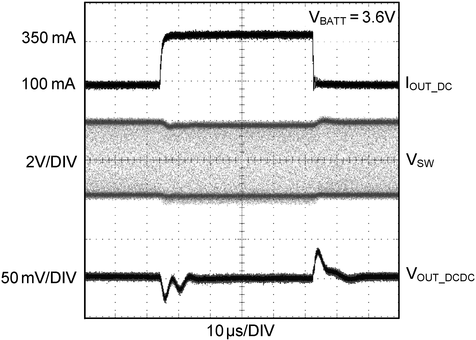
| PWM Mode: 100 mA to 350 mA |
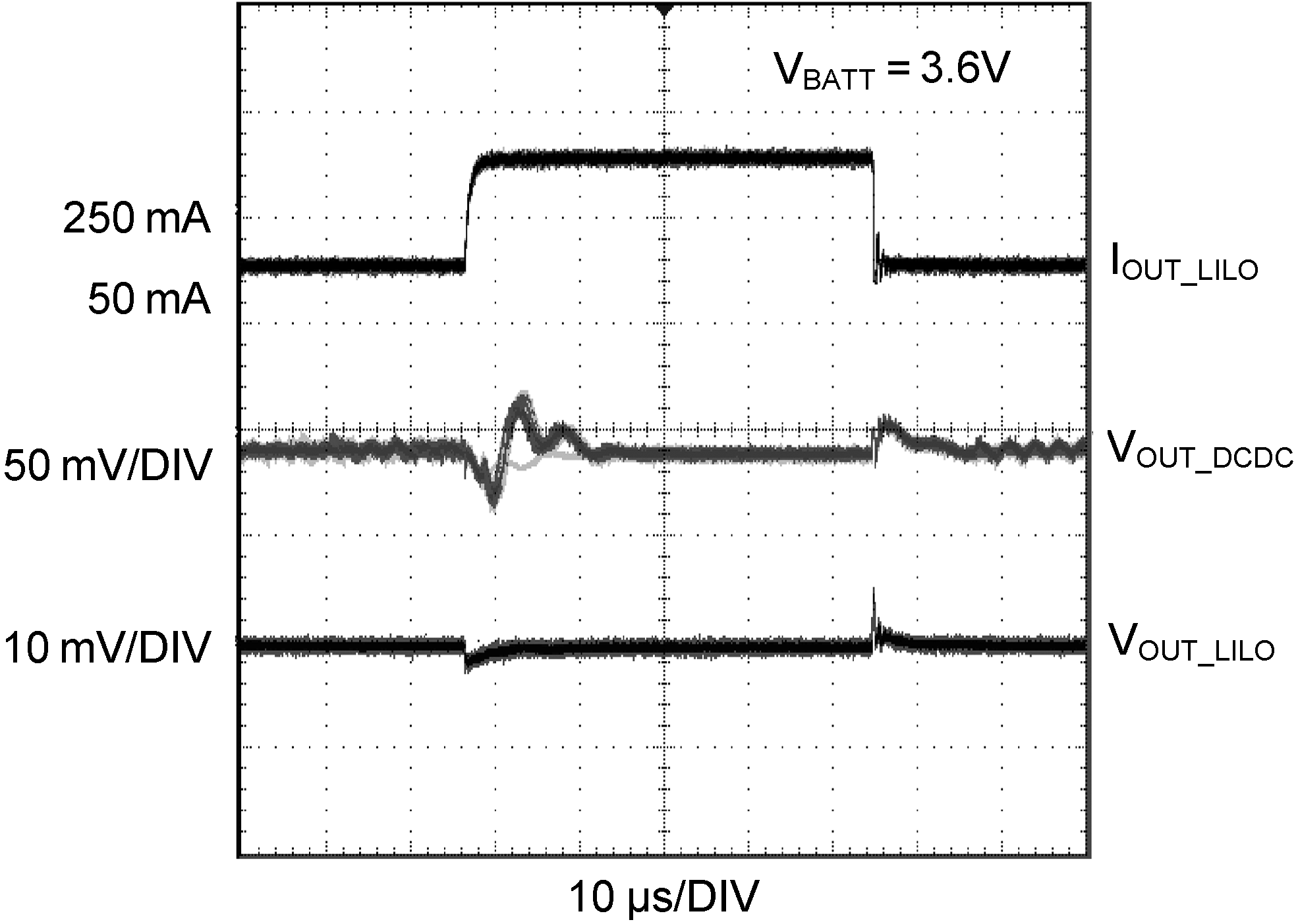
| LILO 50 mA to 250 mA |
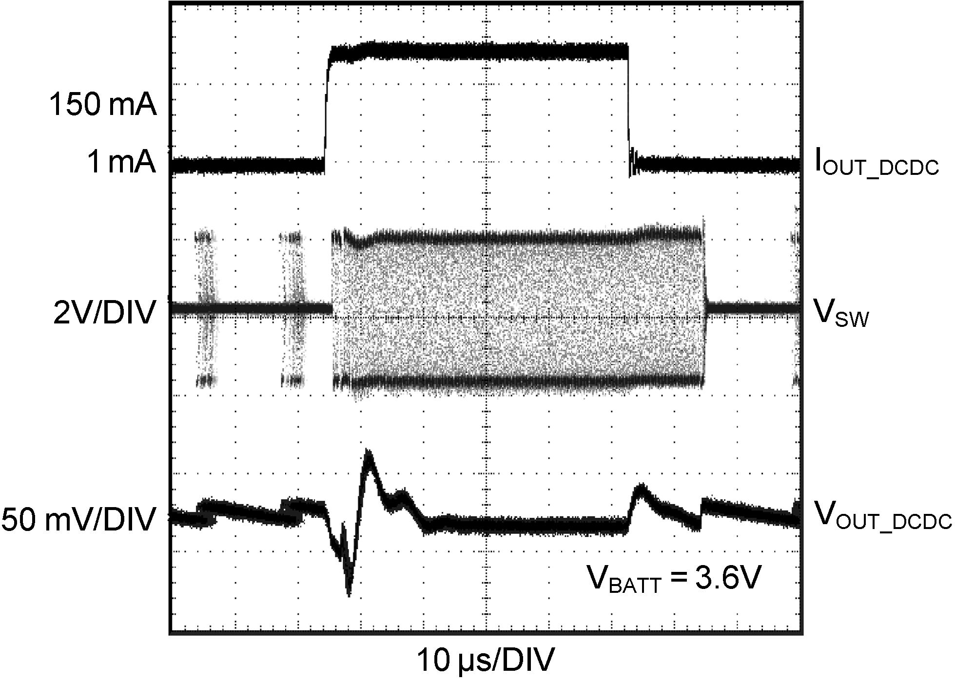
| PFM Mode: 1 mA to 150 mA |
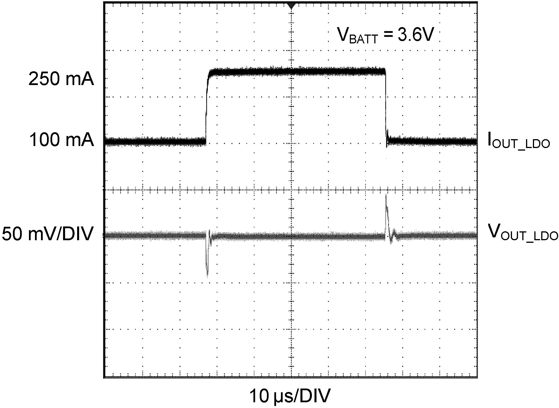
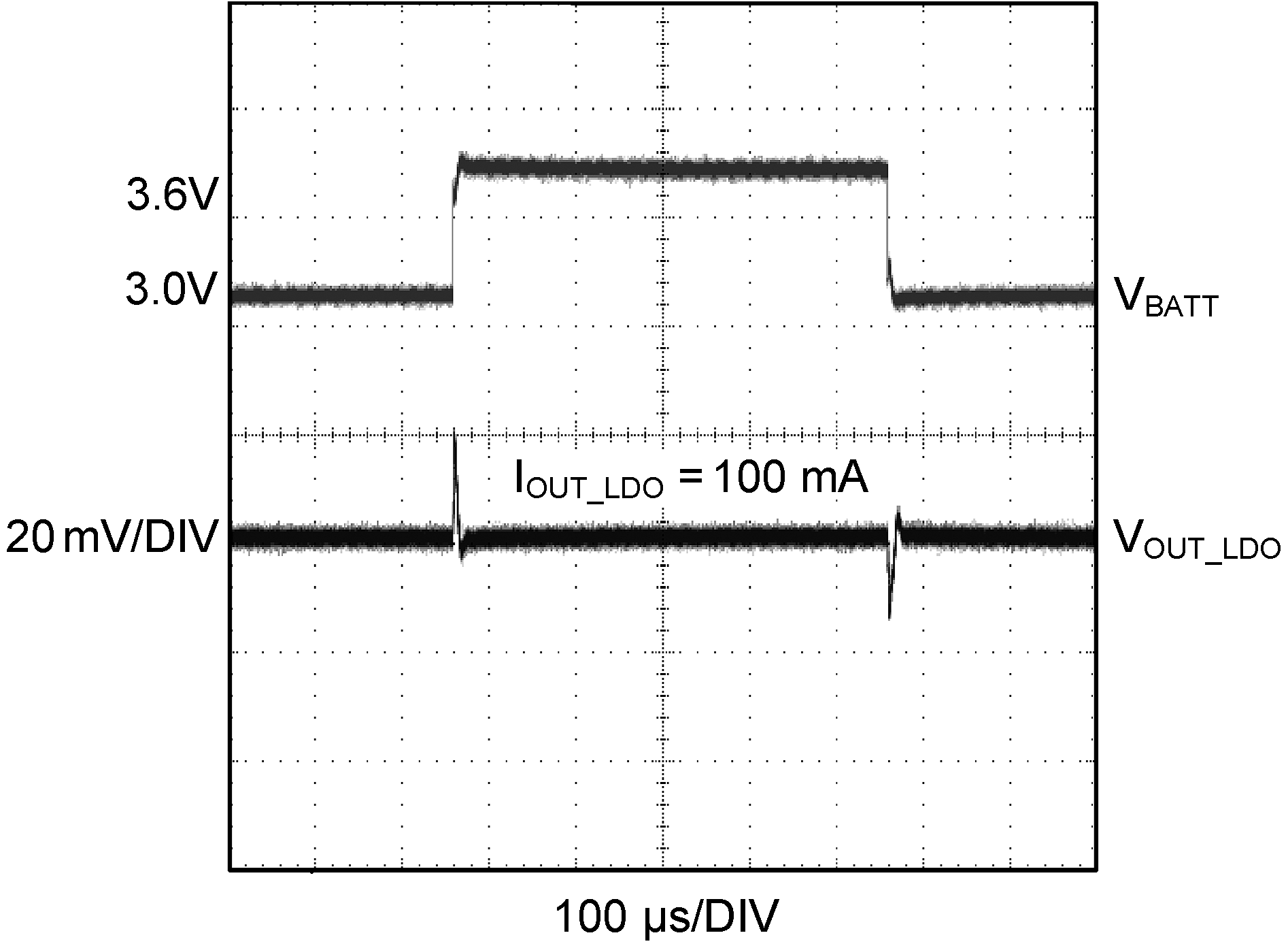
| LDO 100 mA to 250 mA |