SNVS520F August 2008 – November 2016 LM3686
PRODUCTION DATA.
- 1 Features
- 2 Applications
- 3 Description
- 4 Revision History
- 5 Description (Continued)
- 6 Pin Configuration and Functions
-
7 Specifications
- 7.1 Absolute Maximum Ratings
- 7.2 ESD Ratings
- 7.3 Recommended Operating Conditions
- 7.4 Thermal Information
- 7.5 Electrical Characteristics: Linear Regulator - LILO
- 7.6 Electrical Characteristics: Linear Regulator - LDO
- 7.7 Electrical Characteristics: DC-DC Converter
- 7.8 Electrical Characteristics: Global Parameters (DCDC, LILO, and LDO)
- 7.9 Typical Characteristics
- 8 Detailed Description
- 9 Application and Implementation
- 10Power Supply Recommendations
- 11Layout
- 12Device and Documentation Support
- 13Mechanical, Packaging, and Orderable Information
8 Detailed Description
8.1 Overview
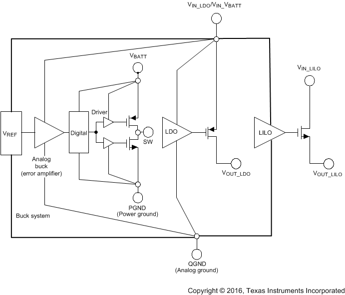
The LM3686 incorporates a high efficiency synchronous switching step-down DC-DC converter, a very low dropout linear regulator (LILO), and ultra-low-noise linear regulator.
The DC-DC converter delivers a constant voltage from a single Li- Ion battery and input voltage rails from 2.7 V to 5.5 V to portable devices such as cell phones and PDAs. Using a voltage mode architecture with synchronous rectification, it has the ability to deliver up to 600-mA load current (when not powering the LILO) depending on the input voltage, output voltage, ambient temperature, and the inductor chosen.
The linear regulator delivers a constant voltage biased from VIN_LILO power input typically the output voltage of the DC-DC converter is used (post regulation) with a maximum load current of 350 mA.
The other linear regulator delivers a constant voltage biased from VIN_LDO power input with a maximum load current of 300 mA.
Three enable pins allow the independent control of the three outputs. Shutdown mode turns off the device, offering the lowest current consumption (ISHUTDOWN = 2.5 µA typical).
Besides the shutdown feature, there are two more modes of operation for the DC-DC converter, depending on the current required:
- Pulse width modulation (PWM) and
- Pulse frequency modulation (PFM).
The device operates in PWM mode at load current of approximately 80 mA or higher. Lighter load current cause the device to automatically switch into PFM for reduced current consumption (IQ_VBATT = 28 µA typical) and a longer battery life.
Additional features include soft-start, start-up mode of the linear regulator, undervoltage protection, current overload protection, and overtemperature protection.
An internal reference generates a 1.8-V biasing an internal resistive divider to create a reference voltage range from 0.7 V to 1.8 V (in 50-mV steps) for the LILO and the 0.5-V reference used for the DC-DC converter. The ultra-low-noise linear regulator also has internal reference that generates a 1.8-V biasing for a internal resistor divider, thus creating a reference voltage ranging from 1.5 V to 3.3 V.
The undervoltage lockout feature enables the device to start-up once VBATT has reached 2.65 V typically and turns the device off if VBATT drops below 2.41 V typically.
NOTE
Post regulation: When the DC-DC converter is switched off while the linear regulator is still enabled, the LILO can still support up to 50 mA. The linear regulator LILO is turned on via a small NMOS device supplied by VIN_LDO . The maximum current is 50 mA when this small NMOS is ON. If higher current > 50 mA is desired the following condition must be met:
- EN_DC = HIGH
When the condition is met, the LILO transitions to the large NMOS and can support up to 350 mA.
8.2 Functional Block Diagram
8.3 Feature Description
8.3.1 DC-DC Converter Operation
During the first part of each switching cycle, the control block in the LM3686 turns on the internal PFET switch. This allows current to flow from the input VBATT through the switch pin SW and the inductor to the output filter capacitor and load. The inductor limits the current to a ramp with a slope of (VBATT – VOUT_DCDC) / L, by storing energy in the magnetic field.
During the second part of each cycle, the controller turns the PFET switch off, blocking current flow from the input, and then turns the NFET synchronous rectifier on. The inductor draws current from ground through the NFET to the output filter capacitor and load, which ramps the inductor current down with a slope of (– VOUT_DCDC / L).
The output filter stores charge when the inductor current is high, and releases it when low, smoothing the voltage across the load.
The output voltage is regulated by modulating the PFET switch on time to control the average current sent to the load. The effect is identical to sending a duty-cycle modulated rectangular wave formed by the switch and synchronous rectifier at the SW pin to a low-pass filter formed by the inductor and output filter capacitor. The output voltage is equal to the average voltage at the SW pin.
8.3.1.1 PWM Operation
During pulse width modulation (PWM) operation the converter operates as a voltage-mode controller with input voltage feed forward. This allows the converter to achieve good load and line regulation. The DC gain of the power stage is proportional to the input voltage. To eliminate this dependency, feed forward inversely proportional to the input voltage is introduced.
While in PWM mode, the output voltage is regulated by switching at a constant frequency and then modulating the energy per cycle to control power to the load. At the beginning of each clock cycle the PFET switch is turned on and the inductor current ramps up until the duty-cycle comparator trips and the control logic turns off the switch. The current limit comparator can also turn off the switch in case the current limit of the PFET is exceeded. Then the NFET switch is turned on and the inductor current ramps down. The next cycle is initiated by the clock turning off the NFET and turning on the PFET.
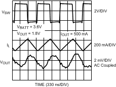 Figure 11. Typical PWM Operation
8.3.1.2 PFM Operation
At very light load, the DC-DC converter enters PFM mode and operates with reduced switching frequency and supply current to maintain high efficiency. The part automatically transitions into PFM mode when either of two conditions occurs for a duration of 32 or more clock cycles:
- The NFET current reaches zero.
- The peak PMOS switch current drops below the IMODE level, (typically IMODE < 75 mA + VBATT / 55 Ω ).
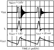 Figure 12. Typical PFM Operation
During PFM operation, the DC-DC converter positions the output voltage slightly higher than the nominal output voltage during PWM operation, allowing additional headroom for voltage drop during a load transient from light to heavy load. The PFM comparators sense the output voltage via the feedback pin and control the switching of the output FETs such that the output voltage ramps between approximately 0.2% and approximately 1.8% above the nominal PWM output voltage. If the output voltage is below the high PFM comparator threshold, the PMOS power switch is turned on. It remains on until the output voltage reaches the high PFM threshold or the peak current exceeds the IPFM level set for PFM mode. The typical peak current in PFM mode is: IPFM = 112 mA + VBATT / 20 Ω.
Once the PMOS power switch is turned off, the NMOS power switch is turned on until the inductor current ramps to zero. When the NMOS zero-current condition is detected, the NMOS power switch is turned off. If the output voltage is below the high PFM comparator threshold (see Figure 13), the PMOS switch is again turned on and the cycle is repeated until the output reaches the desired level. Once the output reaches the high PFM threshold, the NMOS switch is turned on briefly to ramp the inductor current to zero. Both output switches are then turned off, and the device enters an extremely low power mode. Quiescent supply current during this sleep mode is 28 µA (typical), which allows the part to achieve high efficiency under extremely light load conditions.
If the load current should increase during PFM mode (see Figure 13) causing the output voltage to fall below the low2 PFM threshold, the part automatically transitions into fixed-frequency PWM mode.
When VBATT = 2.7 V the device transitions from PWM to PFM mode at approximately 35 mA output current and from PFM mode to PWM mode at approximately 95 mA. When VBATT= 3.6 V, PWM-to-PFM transition happens at approximately 42 mA and PFM-to-PWM transition happens at approximately 115 mA. When VBATT = 4.5 V, PWM-to-PFM transition happens at approximately 60 mA and PFM-to-PWM transition happens at approximately 135 mA.
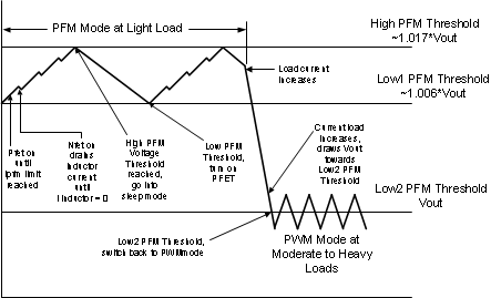 Figure 13. Operation In PFM Mode and Transfer to PWM Mode
8.3.1.3 Internal Synchronous Rectification
While in PWM mode, the DC-DC converter uses an internal NFET as a synchronous rectifier to reduce rectifier forward voltage drop and associated power loss. Synchronous rectification provides a significant improvement in efficiency whenever the output voltage is relatively low compared to the voltage drop across an ordinary rectifier diode.
8.3.1.4 Current Limiting
A current limit feature allows the LM3686 to protect itself and external components during overload conditions. PWM mode implements current limiting using an internal comparator that trips at 1220 mA (typical). If the output is shorted to ground the device enters a timed current limit mode where the NFET is turned on for a longer duration until the inductor current falls below a low threshold. This allows the inductor current more time to decay, thereby preventing runaway.
8.3.1.5 Soft Start
The DC-DC converter has a soft-start circuit that limits in-rush current during start-up. During start-up the switch-current limit is increased in steps. Soft start is activated only if EN_DCDC goes from logic low to logic high after VBATT reaches 2.7 V. Soft start is implemented by increasing switch current limit in steps of 200 mA, 400 mA, 600 mA and 1220 mA (typical switch current limit). The start-up time thereby depends on the output capacitor and load current demanded at start-up. Typical start-up times with a 10 µF output capacitor and 200 mA load is 350 µs and with 1 mA load is 200 µs.
8.3.2 Linear Regulator Operation (LILO)
In a typical post-regulation application the power input voltage VIN_LILO for the linear regulator is generated by the DC-DC converter. Using a buck converter to reduce the battery voltage to a lower input voltage for the linear regulator translates to higher efficiency and lower power dissipation.
It is also possible to operate the linear regulator independent of the DC-DC converter output voltage either from VIN_LDO/VBATT or from a different source (VIN_LILO) – (IOUT_LILO = 50 mA maximum in independent mode).
An input capacitor of 1 µF at VIN_LILO is needed to be added if no other filter or bypass capacitor is present in the VIN_LILO path.
8.3.2.1 Start-up Mode
If VIN_LILO > VOUT_LILO(NOM) + 250 mV the main regulator is active, offering a rated output current of 350 mA and supplied by VIN_LILO (large NMOS).
If VIN_LILO < VOUT_LILO(NOM) + 150 mV the start-up LILO is active, providing a reduced rated output current of 50 mA typical, supplied by VBATT (small NMOS).
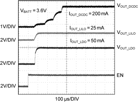 Figure 14. Start-Up Sequence, VEN_DCDC = VEN_LILO = V EN_LDO = VBATT
8.3.3 Current Limiting (LDO and LILO)
The LM3686 incorporates also a current limit for the LDO and LILO to protect itself and external components during overload conditions at their outputs. In the event of a peak overcurrent condition at VOUT_LDO or VOUT_LILO , the output current through the NFET pass device is limited.
8.4 Device Functional Modes
Table 1. Enable Combinations
| EN_DCDC | EN_LILO | EN_LDO | FUNCTION |
|---|---|---|---|
| 0 | 0 | 0 | No outputs |
| 0 | 0 | 1 | Linear regulator enabled only (EN_LDO), supply from VIN_LDO, IOUT_MAX = 300 mA |
| 0 | 1 | 0 | Linear regulator enabled only LILO supplies from VIN_LDO, IOUT_MAX = 50 mA, VIN_LDO > = VOUT_LILO |
| 1 | 0 | 0 | DC-DC converter enabled only |
| 1 | 1 | 0 | Linear regulator and DC-DC enabled |
| 1 | 1 | 1 | DC-DC converter and linear regulator active. Linear regulator starts after DC-DC converter. |
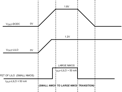 Figure 15. Mode Transition