SNVSAF2A February 2016 – February 2016 LM36922H
PRODUCTION DATA.
- 1 Features
- 2 Applications
- 3 Description
- 4 Revision History
- 5 Pin Configuration and Functions
- 6 Specifications
-
7 Detailed Description
- 7.1 Overview
- 7.2 Functional Block Diagram
- 7.3 Feature Description
- 7.4
Device Functional Modes
- 7.4.1 Brightness Control Modes
- 7.4.2 Boost Switching Frequency
- 7.4.3 Auto-Switching Frequency
- 7.4.4 I2C Address Select (ASEL)
- 7.4.5
Fault Protection/Detection
- 7.4.5.1
Overvoltage Protection (OVP)
- 7.4.5.1.1 Case 1 OVP Fault Only (OVP Threshold Hit and All Enabled Current Sink Inputs > 40 mV)
- 7.4.5.1.2 Case 2a OVP Fault and Open LED String Fault (OVP Threshold Occurrence and Any Enabled Current Sink Input ≤ 40 mV)
- 7.4.5.1.3 Case 2b OVP Fault and Open LED String Fault (OVP Threshold Duration and Any Enabled Current Sink Input ≤ 40 mV)
- 7.4.5.1.4 OVP/LED Open Fault Shutdown
- 7.4.5.1.5 Testing for LED String Open
- 7.4.5.2 Voltage Limitations on LED1, LED2
- 7.4.5.3 LED String Short Fault
- 7.4.5.4 Overcurrent Protection (OCP)
- 7.4.5.5 Device Overtemperature
- 7.4.5.1
Overvoltage Protection (OVP)
- 7.5 Programming
- 7.6 Register Maps
- 8 Applications and Implementation
- 9 Power Supply Recommendations
- 10Layout
- 11Device and Documentation Support
- 12Mechanical, Packaging, and Orderable Information
7 Detailed Description
7.1 Overview
The LM36922H is an inductive boost plus two current sinks white-LED driver designed for powering from one to two strings of white LEDs used in display backlighting. The device operates over the 2.5-V to 5.5-V input voltage range. The 11-bit LED current is set via an I2C interface, via a logic level PWM input, or a combination of both.
7.2 Functional Block Diagram
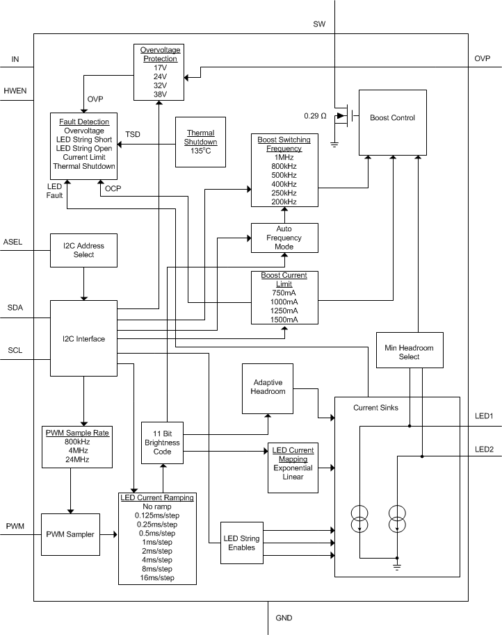
7.3 Feature Description
7.3.1 Enabling the LM36922H
The LM36922H has a logic level input HWEN which serves as the master enable/disable for the device. When HWEN is low the device is disabled, the registers are reset to their default state, the I2C bus is inactive, and the device is placed in a low-power shutdown mode. When HWEN is forced high the device is enabled, and I2C writes are allowed to the device.
7.3.1.1 Current Sink Enable
Each current sink in the device has a separate enable input. This allows for a 1-string or 2-string application. The default is with two strings enabled. Once the correct LED string configuration is programmed, the device can be enabled by writing the chip enable bit high (register 0x10 bit[0]), and then either enabling PWM and driving PWM high, or writing a non-zero code to the brightness registers.
The default setting for the device is with the chip enable bit set to 1, PWM input enabled, and the device in linear mapped mode. Therefore, on power up once HWEN is driven high, the device enters the standby state and actively monitors the PWM input. After a non-zero PWM duty cycle is detected the LM36922H converts the duty cycle information to the linearly weighted 11-bit brightness code. This allows for operation of the device in a stand-alone configuration without the need for any I2C writes. Figure 15 and Figure 16 describe the start-up timing for operation with both PWM controlled current and with I2C controlled current.
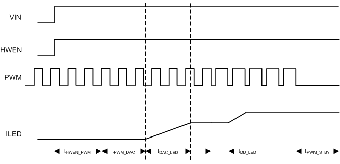 Figure 15. Enabling the LM36922H via PWM
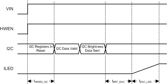 Figure 16. Enabling the LM36922H via I2C
7.3.2 LM36922H Start-Up
The LM36922H can be enabled or disabled in various ways. When disabled, the device is considered shutdown, and the quiescent current drops to ISHDN. When the device is in standby, it returns to the ISHDN current level retaining all programmed register values. Table 1 describes the different operating states for the LM36922H.
Table 1. LM36922H Operating Modes
| LED STRING ENABLES 0x10 bits[2:1] |
PWM INPUT | I2C BRIGHTNESS REGISTERS 0x18 bits[2:0] 0x19 bits[7:0] |
BRIGHTNESS MODE 0x11 bits[6:5] |
DEVICE ENABLE 0x10 bit[0] |
LED CURRENT | |
|---|---|---|---|---|---|---|
| (EXP MAPPING) 0x11 bit[7] = 1 |
(LIN MAPPING) 0x11 bit[7] = 0 |
|||||
| XXX | X | XXX | XX | 0 | Off, device disabled | |
| 0 | X | XXX | XX | 1 | Off, device standby | |
| At least one enabled | X | 0 | 00 | 1 | Off, device in standby | |
| At least one enabled | X | Code > 000 | 00 | 1 | ILED = 50 µA × 1.003040572Code
See(1) |
LED = 37.806 µA + 12.195 µA × Code See(1) |
| At least one enabled | 0 | XXX | 01 | 1 | Off, device in standby | |
| At least one enabled | PWM Signal | XXX | 01 | 1 | ILED = 50 µA × 1.003040572CodeSee(1) | LED = 37.806 µA + 12.195 µA × Code See(1) |
| At least one enabled | 0 | XXX | 10 or 11 | 1 | Off, device in standby | |
| At least one enabled | X | 0 | 10 or 11 | 1 | Off, device in standby | |
| At least one enabled | PWM Signal | Code > 000 | 10 or 11 | 1 | ILED = 50 µA × 1.003040572CodeSee(1) | LED = 37.806 µA + 12.195 µA × Code See(1) |
7.3.3 Brightness Mapping
There are two different ways to map the brightness code (or PWM duty cycle) to the LED current: linear and exponential mapping.
7.3.3.1 Linear Mapping
For linear mapped mode the LED current increases proportionally to the 11-bit brightness code and follows the relationship:

This is valid from codes 1 to 2047. Code 0 programs 0 current. Code is an 11-bit code that can be the I2C brightness code, the digitized PWM duty cycle, or the product of the two.
7.3.3.2 Exponential Mapping
In exponential mapped mode the LED current follows the relationship:

This results in an LED current step size of approximately 0.304% per code. This is valid for codes from 1 to 2047. Code 0 programs 0 current. Code is an 11-bit code that can be the I2C brightness code, the digitized PWM duty cycle, or the product of the two. Figure 17 details the LED current exponential response.
The 11-bit (0.304%) per code step is small enough such that the transition from one code to the next in terms of LED brightness is not distinguishable to the eye. This therefore gives a perfectly smooth brightness increase between adjacent codes.
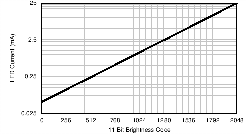 Figure 17. LED Current vs Brightness Code (Exponential Mapping)
7.3.4 PWM Input
The PWM input is a sampled input which converts the input duty cycle information into an 11-bit brightness code. The use of a sampled input eliminates any noise and current ripple that traditional PWM controlled LED drivers are susceptible to.
The PWM input uses logic level thresholds with VIH_MIN = 1.25 V and VIL_MAX = 0.4 V. Because this is a sampled input, there are limits on the max PWM input frequency as well as the resolution that can be achieved.
7.3.4.1 PWM Sample Frequency
There are four selectable sample rates for the PWM input. The choice of sample rate depends on three factors:
- Required PWM Resolution (input duty cycle to brightness code, with 11 bits max)
- PWM Input Frequency
- Efficiency
7.3.4.1.1 PWM Resolution and Input Frequency Range
The PWM input frequency range is 50 Hz to 50 kHz. To achieve the full 11-bit maximum resolution of PWM duty cycle to the LED brightness code (BRT), the input PWM duty cycle must be ≥ 11 bits, and the PWM sample period (1/ƒSAMPLE) must be smaller than the minimum PWM input pulse width. Figure 18 shows the possible brightness code resolutions based on the input PWM frequency. The minimum PWM frequency for each PWM sample rate is described in PWM Timeout.
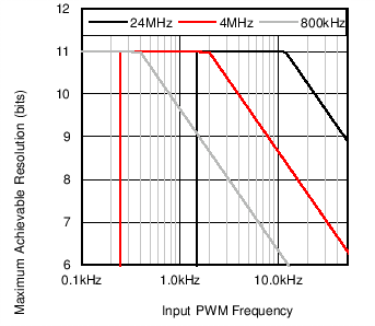 Figure 18. PWM Sample Rate, Resolution, and PWM Input Frequency
7.3.4.1.2 PWM Sample Rate and Efficiency
Efficiency is maximized when the lowest ƒSAMPLE is chosen as this lowers the quiescent operating current of the device. Table 2 describes the typical efficiency tradeoffs for the different sample clock settings.
Table 2. PWM Sample Rate Trade-Offs
| PWM SAMPLE RATE (ƒSAMPLE) | TYPICAL INPUT CURRENT, DEVICE ENABLED ILED = 10 mA/string, 2 × 7 LEDs |
TYPICAL EFFICIENCY | ||
|---|---|---|---|---|
| (0x12 Bits[7:6]) | ƒSW = 1 MHz | VIN = 3.7 V | ||
| 0 | 1.03 mA | 89.7% | ||
| 1 | 1.05 mA | 89.6% | ||
| 1X | 1.35 mA | 89.4% | ||
7.3.4.1.2.1 PWM Sample Rate Example
The number of bits of resolution on the PWM input varies according to the PWM Sample rate and PWM input frequency.
Table 3. PWM Resolution vs PWM Sample Rate
| PWM FREQUENCY (kHz) | RESOLUTION (PWM SAMPLE RATE = 800 kHz) |
RESOLUTION (PWM SAMPLE RATE = 4 MHz) |
RESOLUTION (PWM SAMPLE RATE = 24 MHz) |
|
|---|---|---|---|---|
| 0.4 | 11 | 11 | 11 | |
| 2 | 8.6 | 11 | 11 | |
| 12 | 6.1 | 8.4 | 11 | |
7.3.4.2 PWM Hysteresis
To prevent jitter at the input PWM signal from feeding through the PWM path and causing oscillations in the LED current, the LM36922H offers seven selectable hysteresis settings. The hysteresis works by forcing a specific number of 11-bit LSB code transitions to occur in the input duty cycle before the LED current changes. Table 4 describes the hysteresis. The hysteresis only applies during the change in direction of brightness currents. Once the change in direction has taken place, the PWM input must over come the required LSB(s) of the hysteresis setting before the brightness change takes effect. Once the initial hysteresis has been overcome and the direction in brightness change remains the same, the PWM to current response changes with no hysteresis.
Table 4. PWM Input Hysteresis
| HYSTERESIS SETTING (0x12 Bits[4:2]) | MIN CHANGE IN PWM PULSE WIDTH (Δt) REQUIRED TO CHANGE LED CURRENT, AFTER DIRECTION CHANGE (for ƒPWM < 11.7 kHz) |
MIN CHANGE IN PWM DUTY CYCLE (ΔD) REQUIRED TO CHANGE LED CURRENT AFTER DIRECTION CHANGE | MIN (ΔILED), INCREASE FOR INITIAL CODE CHANGE | |
|---|---|---|---|---|
| EXPONENTIAL MODE | LINEAR MODE | |||
| 000 (0 LSB) | 1/(ƒPWM × 2047) | 0.05% | 0.30% | 0.05% |
| 001 (1 LSB) | 1/(ƒPWM × 1023) | 0.10% | 0.61% | 0.10% |
| 010 (2 LSBs) | 1/(ƒPWM × 511) | 0.20% | 1.21% | 0.20% |
| 011 (3 LSBs) | 1/(ƒPWM × 255) | 0.39% | 2.40% | 0.39% |
| 100 (4 LSBs) | 1/(ƒPWM × 127) | 0.78% | 4.74% | 0.78% |
| 101 (5 LSBs) | 1/(ƒPWM × 63) | 1.56% | 9.26% | 1.56% |
| 110 (6 LSBs) | 1/(ƒPWM × 31) | 3.12% | 17.66% | 3.12% |
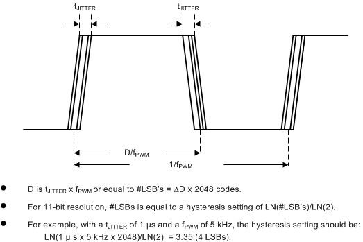 Figure 19. PWM Hysteresis Example
7.3.4.3 PWM Step Response
The LED current response due to a step change in the PWM input is approximately 2 ms to go from minimum LED current to maximum LED current.
7.3.4.4 PWM Timeout
The LM36922H PWM timeout feature turns off the boost output when the PWM is enabled and there is no PWM pulse detected. The timeout duration changes based on the PWM Sample Rate selected which results in a minimum supported PWM input frequency. The sample rate, timeout, and minimum supported PWM frequency are summarized in Table 5.
Table 5. PWM Timeout and Minimum Supported PWM Frequency vs PWM Sample Rate
| SAMPLE RATE | TIMEOUT | MINIMUM SUPPORTED PWM FREQUENCY | ||
|---|---|---|---|---|
| 0.8 MHz | 25 msec | 48 Hz | ||
| 4 MHz | 3 msec | 400 Hz | ||
| 24 MHz | 0.6 msec | 2000 Hz | ||
7.3.5 LED Current Ramping
There are 8 programmable ramp rates available in the LM36922H. These ramp rates are programmable as a time per step. Therefore, the ramp time from one current set-point to the next, depends on the number of code steps between currents and the programmed time per step. This ramp time to change from one brightness set-point (Code A) to the next brightness set-point (Code B) is given by:

For example, assume the ramp is enabled and set to 1 ms per step. Additionally, the brightness code is set to 0x444 (1092d). Then the brightness code is adjusted to 0x7FF (2047d). The time the current takes to ramp from the initial set-point to max brightness is:

7.3.6 Regulated Headroom Voltage
In order to optimize efficiency, current accuracy, and string-to-string matching the LED current sink regulated headroom voltage (VHR) varies with the target LED current. Figure 20 details the typical variation of VHR with LED current. This allows for increased solution efficiency as the dropout voltage of the LED driver changes. Furthermore, in order to ensure that both current sinks remain in regulation whenever there is a mismatch in string voltages, the minimum headroom voltage between VLED1, VLED2 becomes the regulation point for the boost converter. For example, if the LEDs connected to LED1 require 12 V, the LEDs connected to LED2 require 12.5 V at the programmed current, then the voltage at LED1 is VHR + 0.5 V and the voltage at LED2 is VHR. In other words, the boost makes the cathode of the highest voltage LED string the regulation point.
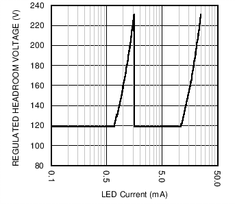 Figure 20. LM36922H Typical Exponential Regulated Headroom Voltage vs Programmed LED Current
7.4 Device Functional Modes
7.4.1 Brightness Control Modes
The LM36922H has four brightness control modes:
- I2C Only (brightness mode 00)
- PWM Only (brightness mode 01)
- I2C × PWM with ramping only between I2C codes (brightness mode 10)
- I2C × PWM with ramping between I2C × PWM changes (brightness mode 11)
7.4.1.1 I2C Only (Brightness Mode 00)
In brightness control mode 00 the I2C Brightness registers are in control of the LED current, and the PWM input is disabled. The brightness data (BRT) is the concatenation of the two brightness registers (3 LSBs) and (8 MSBs) (registers 0x18 and 0x19, respectively). The LED current only changes when the MSBs are written, meaning that to do a full 11-bit current change via I2C, first the 3 LSBs are written and then the 8 MSBs are written. In this mode the ramper only controls the time from one I2C brightness set-point to the next (see Figure 21).
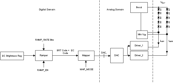 Figure 21. Brightness Control 00 (I2C Only)
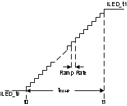
- At time t0 the I2C Brightness Code is changed from 0x444 (1092d) to 0x7FF (2047d)
- Ramp Rate programmed to 1ms/step
- Mapping Mode set to Linear
- ILED_t0 = 1092 × 12.213 µA = 13.337 mA
- ILED_t1 = 2047 × 12.213 µA = 25 mA
- tRAMP = (t1 – t0) = 1ms/step × (2047 – 1092 – 1) = 954 ms
7.4.1.2 PWM Only (Brightness Mode 01)
In brightness mode 01, only the PWM input sets the brightness. The I2C code is ignored. The LM36922H samples the PWM input and determines the duty cycle; this measured duty cycle is translated into an 11-bit digital code. The resultant code is then applied to the internal ramper (see Figure 23).
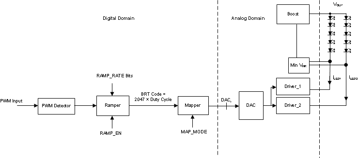 Figure 23. Brightness Control 01 (PWM Only)

- At time t0 the PWM duty cycle changed from 25% to 100%
- Ramp Rate programmed to 1 ms/step
- Mapping Mode set to Linear
- ILED_t0 = 25 mA × 0.25 = 6.25 mA
- ILED_t1 = 25 mA × 1 = 25 mA
- tRAMP = (t1 – t0) = 1 ms/step × (2047 × 1 – 2047 × 0.25 – 1) = 1534 ms
7.4.1.3 I2C + PWM Brightness Control (Multiply Then Ramp) Brightness Mode 10
In brightness control mode 10 the I2C Brightness register and the PWM input are both in control of the LED current. In this case the I2C brightness code is multiplied with the PWM duty cycle to produce an 11-bit code which is then sent to the ramper. In this mode ramping is achieved between I2C and PWM currents (see Figure 25).
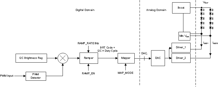 Figure 25. Brightness Control 10 (I2C + PWM)

- At time t0 the I2C Brightness code changed from 0x444 (1092d) to 0x7FF (2047d)
- At time t0 the PWM duty cycle changed from 50% to 75%
- Ramp Rate programmed to 1ms/step
- Mapping Mode set to Linear
- ILED_t0 = 1092 × 12.213 µA × 0.5 = 6.668 mA
- ILED_t1 = 2047 × 12.213 µA × 0.75 = 18.75 mA
- tRAMP = (t1 – t0) = 1 ms/step × (2047 × 0.75 – 1092 × 0.5 – 1) = 988 ms
7.4.1.4 I2C + PWM Brightness Control (Ramp Then Multiply) Brightness Mode 11
In brightness control mode 11 both the I2C brightness code and the PWM duty cycle control the LED current. In this case the ramper only changes the time from one I2C brightness code to the next. The PWM duty cycle is multiplied with the I2C brightness code at the output of the ramper (see Figure 27).
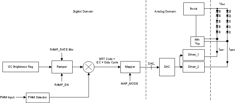 Figure 27. Brightness Control 11 (I2C + PWM)
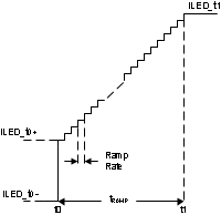
- At time t0 the I2C Brightness code changed from 0x444 (1092d) to 0x7FF (2047d)
- At time t0 the PWM duty cycle changed from 50% to 75%
- Ramp Rate programmed to 1 ms/step
- Mapping Mode set to Linear
- ILED_t0– = 1092 × 12.213 µA × 0.5 = 6.668 mA
- ILED_t0+ = 1092 × 12.213 µA × 0.75 = 10.002 mA
- tRAMP = (t1 – t0) = 1 ms/step × (2047 – 1092 – 1) = 954 ms
7.4.2 Boost Switching Frequency
The LM36922H has two programmable switching frequencies: 500 kHz and 1 MHz. These are set via the Boost Control 1 register 0x13 bit [5]. Once the switching frequency is set, this nominal value can be shifted down by 12% via the boost switching frequency shift bit (register 0x13 bit[6]). Operation at 500 kHz is better suited for configurations which use a 10-µH inductor or use the auto-frequency mode and switch over to 500 kHz at lighter loads. Operation at 1 MHz is primarily beneficial at higher output currents, where the average inductor current is much larger than the inductor current ripple. For maximum efficiency across the entire load current range the device incorporates an automatic frequency shift mode (see Auto-Switching Frequency).
7.4.2.1 Minimum Inductor Select
The LM36922H can use inductors in the range of 4.7 µH to 10 µH. In order to optimize the converter response to changes in VIN and load, the Min Inductor Select bit (register 0x13 bit[4]) should be selected depending on which value of inductance is chosen. For 10-µH inductors this bit should be set to 1. For less than 10 µH, this bit should be set to 0.
7.4.3 Auto-Switching Frequency
To take advantage of frequency vs load dependent losses, the LM36922H has the ability to automatically change the boost switching frequency based on the magnitude of the load current. In addition to the register programmable switching frequencies of 500 kHz and 1 MHz, the auto-frequency mode also incorporates a low frequency selection of 250 kHz. It is important to note that the 250-kHz frequency is only accessible in auto-frequency mode and has a maximum boost duty cycle (DMAX) of 50%.
Auto-frequency mode operates by using 2 programmable registers (Auto Frequency High Threshold (register 0x15) and Auto Frequency Low Threshold (0x16)). The high threshold determines the switchover from 1 MHz to 500 kHz. The low threshold determines the switchover from 500 kHz to 250 kHz. Both the High and Low Threshold registers take an 8-bit code which is compared against the 8 MSB of the brightness register (register 0x19). Table 6 details the boundaries for this mode.
Table 6. Auto-Switching Frequency Operation
| BRIGHTNESS CODE MSBs (Register 0x19 bits[7:0]) | BOOST SWITCHING FREQUENCY |
|---|---|
| < Auto Frequency Low Threshold (register 15 Bits[7:0]) | 250 kHz (DMAX = 50%) |
| > Auto Frequency Low Threshold (Register 15 Bits[7:0]) or < Auto Frequency High Threshold (Register 14 Bits[7:0]) | 500 kHz |
| ≥ Auto Frequency High Threshold (register 14 Bits[7:0]) | 1 MHz |
Automatic-frequency mode is enabled whenever there is a non-zero code in either the Auto-Frequency High or Auto-Frequency Low registers. To disable the auto-frequency shift mode, set both registers to 0x00. When automatic-frequency select mode is disabled, the switching frequency operates at the programmed frequency (Register 0x13 bit[5]) across the entire LED current range. provides a guideline for selecting the auto-frequency 250-kHz threshold setting; the actual setting needs to be verified in the application.
Table 7. Auto Frequency 250-kHz Threshold Settings
| CONDITION (Vƒ = 3.2 V, ILED = 25 mA) |
INDUCTOR (µH) | RECOMMENDED AUTO FREQUENCY LOW THRESHOLD MAXIMUM VALUE (NO SHIFT) |
OUTPUT POWER AT AUTO FREQUENCY SWITCHOVER (W) |
|
|---|---|---|---|---|
| 2 × 4 LEDs | 10 | 0x2f | 0.173 | |
| 2 × 5 LEDs | 10 | 0x27 | 0.168 | |
| 2 × 6 LEDs | 10 | 0x21 | 0.178 | |
| 2 × 7 LEDs | 10 | 0x1f | 0.210 | |
| 2 × 8 LEDs | 10 | 0x1b | 0.189 | |
7.4.4 I2C Address Select (ASEL)
The LM36922H provides two I2C slave address options. When ASEL = GND the slave address is set to 0x36. When ASEL = VIN the slave address is set to 0x37. This static input pin is read on power up (VIN > 1.8 V and HWEN > VIH) and must not be changed after power up.
7.4.5 Fault Protection/Detection
7.4.5.1 Overvoltage Protection (OVP)
The LM36922H provides four OVP thresholds (17 V, 24 V, 32 V, and 38 V). The OVP circuitry monitors the boost output voltage (VOUT) and protects OUT and SW from exceeding safe operating voltages in case of open load conditions or in the event the LED string voltage requires more voltage than the programmed OVP setting. The OVP thresholds are programmed in register 13 bits[3:2]. The operation of OVP differentiates between two overvoltage conditions (see Case 1 OVP Fault Only (OVP Threshold Hit and All Enabled Current Sink Inputs > 40 mV), Case 1 OVP Fault Only (OVP Threshold Hit and All Enabled Current Sink Inputs > 40 mV), and Case 2b OVP Fault and Open LED String Fault (OVP Threshold Duration and Any Enabled Current Sink Input ≤ 40 mV)).
7.4.5.1.1 Case 1 OVP Fault Only (OVP Threshold Hit and All Enabled Current Sink Inputs > 40 mV)
In steady-state operation with VOUT near the OVP threshold a rapid change in VIN or brightness code can result in a momentary transient excursion of VOUT above the OVP threshold. In this case the boost circuitry is disabled until VOUT drops below OVP – hysteresis (1 V). Once this happens the boost is re-enabled and steady state regulation continues. If VOUT remains above the OVP threshold for > 1 ms the OVP Flag is set (register 0x1F bit[0]).
7.4.5.1.2 Case 2a OVP Fault and Open LED String Fault (OVP Threshold Occurrence and Any Enabled Current Sink Input ≤ 40 mV)
When any of the enabled LED strings is open the boost converter tries to drive VOUT above OVP and at the same time the open string(s) current sink headroom voltage(s) (LED1, LED2) drop to 0. When the LM36922H detects three occurrences of VOUT > OVP and any enabled current sink input (VLED1 or VLED2) ≤ 40 mV, the OVP Fault flag is set (register 0x1F bit[0]), and the LED Open Fault flag is set (register 0x1F bit[4]).
7.4.5.1.3 Case 2b OVP Fault and Open LED String Fault (OVP Threshold Duration and Any Enabled Current Sink Input ≤ 40 mV)
When any of the enabled LED strings is open the boost converter tries to drive VOUT above OVP and at the same time the open string(s) current sink headroom voltage(s) (LED1, LED2) drop to 0. When the LM36922H detects VOUT > OVP for > 1 msec and any enabled current sink input (VLED1 or VLED2) ≤ 40 mV, the OVP Fault flag is set (register 0x1F bit[0]), and the LED Open Fault flag is set (register 0x1F bit[4]).
7.4.5.1.4 OVP/LED Open Fault Shutdown
The LM36922H has the option of shutting down the device when the OVP flag is set. This option can be enabled or disabled via register 0x1E bit[0]. When the shutdown option is disabled the fault flag is a report only. When the device is shut down due to an OVP/LED String Open fault, the fault flags register must be read back before the LM36922H can be re-enabled.
7.4.5.1.5 Testing for LED String Open
The procedure for detecting an open in a LED string is:
- Apply power the the LM36922H .
- Enable all LED strings (Register 0x10 = 0x07).
- Set maximum brightness (Register 0x18 = 0x07 and Register 0x19 = 0xFF).
- Set the brightness control (Register 0x11 = 0x00).
- Open LED1 string.
- Wait 4 msec.
- Read LED open fault (Register 0x1F).
- If bit[4] = 1, then a LED open fault condition has been detected.
- Connect LED1 string.
- Repeat the procedure for the other LED strings.
7.4.5.2 Voltage Limitations on LED1, LED2
The inputs to current sinks LED1, LED2 are rated for 30 V (absolute maximum voltage). This is lower than the boost output capability as set by the OVP threshold (maximum specification) of 39 V. To ensure that the current sink inputs remain below their absolute maximum rating, the LED configuration between LED1 or LED2 must not have a voltage difference between strings so that VLED1/2 have a voltage greater than 30 V.
7.4.5.3 LED String Short Fault
The LM36922H can detect an LED string short fault. This happens when the voltage between VIN and any enabled current sink input has dropped below (1.5 V). This test can only be performed on one LED string at a time. Performing this test with more than one LED string enabled can result in a faulty reading. The procedure for detecting a short in a LED string is:
- Apply power the LM36922H .
- Enable only LED1 string (Register 0x10 = 0x03).
- Enable short fault (Register 0x1E = 0x01.
- Set maximum brightness (Register 0x18 = 0x07 and Register 0x19 = 0xFF).
- Set the brightness control (Register 0x11 = 0x00).
- Wait 4 msec.
- Read LED short fault (Register 0x1F).
- If bit[3] = 1, then a LED short fault condition has been detected.
- Set chip enable and LED string enable low (Register 0x10 = 0x00).
- Repeat the procedure for the other LED strings.
7.4.5.4 Overcurrent Protection (OCP)
The LM36922H has four selectable OCP thresholds (750 mA, 1000 mA, 1250 mA, and 1500 mA). These are programmable in register 0x13 bits[1:0]. The OCP threshold is a cycle-by-cycle current limit and is detected in the internal low-side NFET. Once the threshold is hit the NFET turns off for the remainder of the switching period.
7.4.5.4.1 OCP Fault
If enough overcurrent threshold events occur, the OCP Flag (register 0x1F bit[1]) is set. To avoid transient conditions from inadvertently setting the OCP Flag, a pulse density counter monitors OCP threshold events over a 128-µs period. If 8 consecutive 128-µs periods occur where the pulse density count has found two or more OCP events,then the OCP Flag is set.
During device start-up and during brightness code changes, there is a 4-ms blank time where OCP events are ignored. As a result, if the device starts up in an overcurrent condition there is an approximate 5-ms delay before the OCP Flag is set.
7.4.5.4.2 OCP Shutdown
The LM36922H has the option of shutting down the device when the OCP flag is set. This option can be enabled or disabled via register 0x1E bit[1]. When the shutdown option is disabled, the fault flag is a report only. When the device is shut down due to an OCP fault, the fault flags register must be read back before the LM36922H can be re-enabled.
7.4.5.5 Device Overtemperature
Thermal shutdown (TSD) is triggered when the device die temperature reaches 135˚C. When this happens the boost stops switching, and the TSD Flag (register 0x1F bit[2]) is set. The boost automatically starts up again when the die temperature cools down to 120°C.
7.4.5.5.1 Overtemperature Shutdown
The LM36922H has the option of shutting down the device when the TSD flag is set. This option can be enabled or disabled via register 0x1E bit[2]. When the shutdown option is disabled the fault flag is a report only. When the device is shutdown due to a TSD fault, the Fault Flags register must be read back before the LM36922H can be re-enabled.
7.5 Programming
7.5.1 I2C Interface
7.5.1.1 Start and Stop Conditions
The LM36922H is configured via an I2C interface. START (S) and STOP (P) conditions classify the beginning and the end of the I2C session Figure 29. A START condition is defined as SDA transitioning from HIGH to LOW while SCL is HIGH. A STOP condition is defined as SDA transitioning from LOW to HIGH while SCL is HIGH. The I2C master always generates the START and STOP conditions. The I2C bus is considered busy after a START condition and free after a STOP condition. During the data transmission the I2C master can generate repeated START conditions. A START and a repeated START conditions are equivalent function-wise. The data on SDA must be stable during the HIGH period of the clock signal (SCL). In other words, the state of SDA can only be changed when SCL is LOW.
 Figure 29. I2C Start and Stop Conditions
7.5.1.2 I2C Address
After the START condition the I2C master sends the 7-bit chip address followed by an eighth bit read or write (R/W). R/W = 0 indicates a WRITE, and R/W = 1 indicates a READ. The second byte following the chip address selects the register address to which the data is written. The third byte contains the data for the selected register.
7.5.1.3 Transferring Data
Every byte on the SDA line must be eight bits long with the most significant bit (MSB) transferred first. Each byte of data must be followed by an acknowledge bit (ACK). The acknowledge related clock pulse, (9th clock pulse), is generated by the master. The master then releases SDA (HIGH) during the 9th clock pulse. The LM36922H pulls down SDA during the 9th clock pulse, signifying an acknowledge. An acknowledge is generated after each byte has been received.
7.5.1.4 Register Programming
For glitch free operation, the following bits and/or registers should only be programmed while the LED Enable bits are 0 (Register 0x10, Bit [2:1] = 0) and Device Enable bit is 1 (Register 0x10, Bit[0] = 1) :
- Register 0x11 Bit[7] (Mapping Mode)
- Register 0x11 Bits[6:5] (Brightness Mode)
- Register 0x11 Bit[4] (Ramp Enable)
- Register 0x11 Bit[3:1] (Ramp Rate)
- Register 0x12 Bits[7:6] (PWM Sample Rate)
- Register 0x12 Bits[5] (PWM Polarity)
- Register 0x12 Bit[3:2] (PWM Hysteresis)
- Register 0x12 Bit[3:2] (PWM Pulse Filter)
- Register 0x15 (auto frequency high threshold)
- Register 0x16 (auto frequency low threshold)
7.6 Register Maps
Note: Read of reserved (R) or write-only register returns 0.
Table 8. Revision (0x00)
| Bits [7:4] | Bits [3:0] |
|---|---|
| R | Revision Code |
Table 9. Software Reset (0x01)
| Bits [7:1] | Software Reset Bit [0] |
|---|---|
| R | 0 = Normal Operation 1 = Device Reset (automatically resets back to 0) |
Table 10. Enable (0x10)
| Bits [7:4] | LED2 Enable Bit [2] |
LED1 Enable Bit [1] |
Device Enable Bit [0] |
|
|---|---|---|---|---|
| R | 0 = Disabled 1 = Enabled (Default) |
0 = Disabled 1 = Enabled (Default) |
0 = Disabled 1 = Enabled (Default) |
|
Table 11. Brightness Control (0x11)
| Mapping Mode Bit [7] |
Brightness Mode Bits [6:5] |
Ramp Enable Bits [4] |
Ramp Rate Bit [3:1] |
Bits [0] | |
|---|---|---|---|---|---|
| 0 = Linear (default) 1 = Exponential |
00 = Brightness Register Only 01 = PWM Duty Cycle Only 10 = Multiply Then Ramp (Brightness Register × PWM) 11 = Ramp Then Multiply (Brightness Register × PWM) (default) |
0 = Ramp Disabled (default) 1 = Ramp Enabled |
000 = 0.125 ms/step (default) 001 = 0.250 ms/step 010 = 0.5 ms/step 011 = 1 ms/step 100 = 2 ms/step 101 = 4 ms/step 110 = 8 ms/step 111 = 16 ms/step |
R | |
Table 12. PWM Control (0x12)
| PWM Sample Rate Bit [7:6] |
PWM Input Polarity Bit [5] |
PWM Hysteresis Bits [4:2] |
PWM Pulse Filter Bit [1:0] |
||
|---|---|---|---|---|---|
| 00 = 800 kHz 01 = 4 MHz 1X = 24 MHz (default) |
0 = Active Low 1 = Active High (default) |
000 = None 001 = 1 LSB 010 = 2 LSBs 011 = 3 LSBs 100 = 4 LSBs (default) 101 = 5 LSBs 110 = 6 LSBs 111 = N/A |
00 = No Filter 01 = 100 ns 10 = 150 ns 11 = 200 ns (default) |
||
Table 13. Boost Control 1 (0x13)
| Reserved Bit [7] |
Boost Switching Frequency Shift Bit [6] |
Boost Switching Frequency Select Bit [5] |
Minimum Inductor Select Bit [4] |
Overvoltage Protection (OVP) Bits [3:2] |
Current Limit (OCP) Bits [1:0] |
||
|---|---|---|---|---|---|---|---|
| N/A | 0 = –12% Shift 1 =No Shift (default) |
0 = 500 kHz 1 = 1 MHz (default) |
0 = 4.7 µH (default) 1 = 10 µH |
00 = 17 V 01 = 24 V 10 = 31 V 11 = 38 V (default) |
00 = 750 mA 01 = 1000 mA 10 = 1250 mA 11 = 1500 mA (default) |
||
Table 14. Auto Frequency High Threshold (0x15)
| Auto Frequency High Threshold (500 kHz to 1000 kHz) Bits [7:0] |
||||
|---|---|---|---|---|
| Compared against the 8 MSBs of 11-bit brightness code (default = 00000000). |
Table 15. Auto Frequency Low Threshold (0x16)
| Auto Frequency High Threshold (250 kHz to 500 kHz) Bits [7:0] |
||||
|---|---|---|---|---|
| Compared against the 8 MSBs of 11-bit brightness code (default = 00000000). |
Table 16. Brightness Register LSBs (0x18)
| Bits [7:3] | I2C Brightness Code (LSB) Bits [2:0] |
||||
|---|---|---|---|---|---|
| R | This is the lower 3 bits of the 11-bit brightness code (default = 111). | ||||
Table 17. Brightness Register MSBs (0x19)
| I2C Brightness Code (MSB) Bits [7:0] |
||||
|---|---|---|---|---|
| This is the upper 8 bits of the 11-bit brightness code (default = 11111111). |
Table 18. Fault Control (0x1E)
| Reserved Bits [7:4] |
LED Short Fault Enable Bit [3] |
TSD Shutdown Disable Bit [2] |
OCP Shutdown Disable Bit [1] |
OVP/LED Open Shutdown Disable Bit [0] |
|
|---|---|---|---|---|---|
| R | 0 = LED Short Fault Detection is disabled (default). 1 = LED Short Fault Detection is enabled |
0 = When the TSD Flag is set, the device is forced into shutdown. 1 = No shutdown (default) |
0 = When the OCP Flag is set, the device is forced into shutdown. 1 = No shutdown (default) |
0 = When the OVP Flag is set, the device is forced into shutdown. 1 = No shutdown (default) |
|
Table 19. Fault Flags (0x1F)
| Reserved Bits [7:5] |
LED Open Fault Bit [4] |
LED Short Fault Bit [3] |
TSD Fault Bit [2] |
OCP Fault Bit [1] |
OVP Fault Bit [0] |
|
|---|---|---|---|---|---|---|
| R | 1 = LED String Open Fault | 1 = LED Short Fault | 1 = Thermal Shutdown Fault | 1 = Current Limit Fault | 1 = Output Overvoltage Fault | |