SNVS049F February 2000 – March 2016 LM4120
PRODUCTION DATA.
7 Detailed Description
7.1 Overview
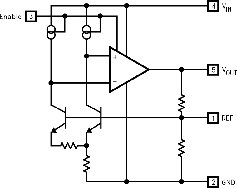
The LM4120 device is a precision bandgap voltage reference available in seven different voltage options with up to 5-mA current source and sink capability. This series reference can operate with input voltages from 2 V to
12 V while consuming 160-µA (typical) supply current. In power-down mode, device current drops to less than
2 μA. The LM4120 is available in two grades, A and Standard.
The best grade devices (A) have an initial accuracy of 0.2% with a TEMPCO of 50 ppm/°C ensured from −40°C to 125°C.
7.2 Functional Block Diagram

7.3 Feature Description
7.3.1 Enable
The ENABLE analog input pin with limited hysteresis generally requires 6 µA (typical) of current to start up the part. During normal operation, the Enable pin must be connected to the VIN pin. There is a minimum slew rate on this pin of about 0.003 V/μs to prevent glitches on the output. All of these conditions can easily be met with ordinary CMOS or TTL logic. The Enable pin can also be used to remotely operate the LM4120 by pulling up the Enable pin voltage to the input voltage level.
When remotely shutting down the LM4120, the Enable pin must be pulled down to the ground. Floating this pin is not recommended.
7.3.2 Reference
The REF pin must remain unconnected in all cases. The reference pin is sensitive to noise, and capacitive loading. Therefore, during the PCB layout care must be taken to keep this pin isolated as much as possible.
7.4 Device Functional Modes
Table 1 describes the functional modes of the LM4120.
Table 1. Enable Pin Mode Summary
| ENABLE PIN CONNECTION | LOGIC STATE | DESCRIPTION |
|---|---|---|
| EN = VIN | 1 | Normal Operation. LM4120 starts up. |
| EN = GND | 0 | LM4120 in shutdown mode |