SNVS020H May 2000 – January 2016 LM431
PRODUCTION DATA.
- 1 Features
- 2 Applications
- 3 Description
- 4 Revision History
- 5 Pin Configuration and Functions
- 6 Specifications
- 7 Parameter Measurement Information
- 8 Detailed Description
- 9 Application and Implementation
- 10Power Supply Recommendations
- 11Layout
- 12Device and Documentation Support
- 13Mechanical, Packaging, and Orderable Information
5 Pin Configuration and Functions
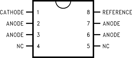
D Package
8-Pin SOIC
Top View

Note: NC = Not internally connected.
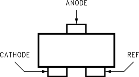
DBZ Package
3-Pin SOT-23
Top View

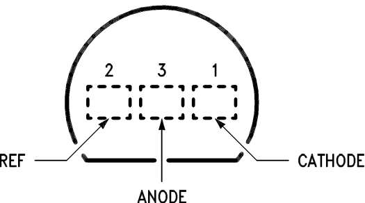
LP Package
3-Pin TO-92
Top View

Pin Functions
| PIN | I/O | DESCRIPTION | |||
|---|---|---|---|---|---|
| NAME | SOIC | SOT-23 | TO-92 | ||
| Anode | 2, 3, 6, 7 | 3 | 3 | O | Anode pin, normally grounded |
| Cathode | 1 | 1 | 1 | I/O | Shunt current/output voltage |
| NC | 4, 5 | — | — | — | No connect |
| Reference | 8 | 2 | 2 | I | Reference pin for adjustable output voltage |