JAJSED5B August   2014  – January 2018 LM43601

PRODUCTION DATA.  

  1. 特長
  2. アプリケーション
  3. 概要
    1.     Device Images
      1.      概略回路図
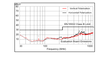
      2.      放射エミッションのグラフ VIN = 12V、VOUT =3.3V、FS = 500kHz、IOUT = 1A
  4. 改訂履歴
  5. Pin Configuration and Functions
    1.     Pin Functions
  6. Specifications
    1. 6.1 Absolute Maximum Ratings
    2. 6.2 ESD Ratings
    3. 6.3 Recommended Operating Conditions
    4. 6.4 Thermal Information
    5. 6.5 Electrical Characteristics
    6. 6.6 Timing Requirements
    7. 6.7 Switching Characteristics
    8. 6.8 Typical Characteristics
  7. Detailed Description
    1. 7.1 Overview
    2. 7.2 Functional Block Diagram
    3. 7.3 Feature Description
      1. 7.3.1  Fixed-Frequency, Peak-Current-Mode Controlled, Step-Down Regulator
      2. 7.3.2  Light Load Operation
      3. 7.3.3  Adjustable Output Voltage
      4. 7.3.4  Enable (ENABLE)
      5. 7.3.5  VCC, UVLO and BIAS
      6. 7.3.6  Soft Start and Voltage Tracking (SS/TRK)
      7. 7.3.7  Switching Frequency (RT) and Synchronization (SYNC)
      8. 7.3.8  Minimum ON-Time, Minimum OFF-Time, and Frequency Foldback at Dropout Conditions
      9. 7.3.9  Internal Compensation and CFF
      10. 7.3.10 Bootstrap Voltage (BOOT)
      11. 7.3.11 Power Good (PGOOD)
      12. 7.3.12 Overcurrent and Short-Circuit Protection
      13. 7.3.13 Thermal Shutdown
    4. 7.4 Device Functional Modes
      1. 7.4.1 Shutdown Mode
      2. 7.4.2 Standby Mode
      3. 7.4.3 Active Mode
      4. 7.4.4 CCM Mode
      5. 7.4.5 Light Load Operation
      6. 7.4.6 Self-Bias Mode
  8. Applications and Implementation
    1. 8.1 Application Information
    2. 8.2 Typical Application
      1. 8.2.1 Design Requirements
      2. 8.2.2 Detailed Design Procedure
        1. 8.2.2.1  Custom Design With WEBENCH® Tools
        2. 8.2.2.2  Output Voltage Setpoint
        3. 8.2.2.3  Switching Frequency
        4. 8.2.2.4  Input Capacitors
        5. 8.2.2.5  Inductor Selection
        6. 8.2.2.6  Output Capacitor Selection
        7. 8.2.2.7  Feedforward Capacitor
        8. 8.2.2.8  Bootstrap Capacitors
        9. 8.2.2.9  VCC Capacitor
        10. 8.2.2.10 BIAS Capacitors
        11. 8.2.2.11 Soft-Start Capacitors
        12. 8.2.2.12 Undervoltage Lockout Set-Point
        13. 8.2.2.13 PGOOD
      3. 8.2.3 Application Curves
  9. Power Supply Recommendations
  10. 10Layout
    1. 10.1 Layout Guidelines
      1. 10.1.1 Compact Layout for EMI Reduction
      2. 10.1.2 Ground Plane and Thermal Considerations
      3. 10.1.3 Feedback Resistors
    2. 10.2 Layout Example
  11. 11デバイスおよびドキュメントのサポート
    1. 11.1 デバイス・サポート
      1. 11.1.1 開発サポート
        1. 11.1.1.1 WEBENCH®ツールによるカスタム設計
    2. 11.2 ドキュメントの更新通知を受け取る方法
    3. 11.3 コミュニティ・リソース
    4. 11.4 商標
    5. 11.5 静電気放電に関する注意事項
    6. 11.6 Glossary
  12. 12メカニカル、パッケージ、および注文情報

パッケージ・オプション

メカニカル・データ(パッケージ|ピン)
サーマルパッド・メカニカル・データ
発注情報

Typical Characteristics

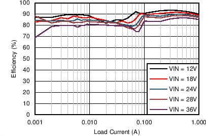
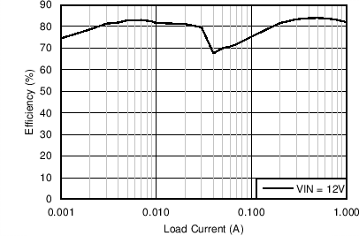
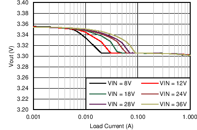
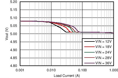
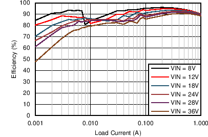
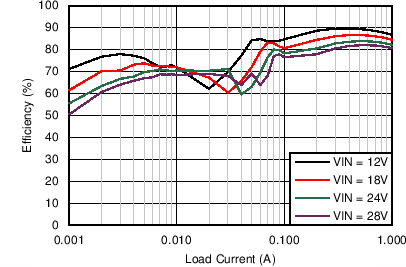
Unless otherwise specified, VIN = 12V, VOUT = 3.3 V, FS = 500 kHz, L = 18 µH, COUT = 100 µF, CFF = 33 pF. See Application Curves for bill of materials (BOM) for other VOUT and FS combinations.
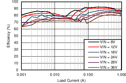
LM43601 C002_Eff_43601_3p3V500k.png
VOUT = 3.3 V FS = 500 kHz
Figure 1. Efficiency
LM43601 C003_Eff_43601_5V500k.png
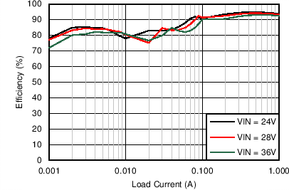
VOUT = 5 V FS = 500 kHz
Figure 3. Efficiency
LM43601 C006_Eff_43601_5V2p2M.png
VOUT = 5 V FS = 2.2 MHz
Figure 5. Efficiency
LM43601 C012_Reg_43601_3p3V500k.png
VOUT = 3.3 V FS = 500 kHz
Figure 7. VOUT Regulation
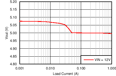
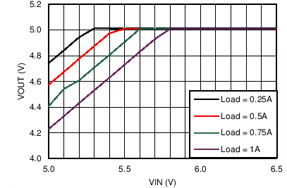
LM43601 C013_Reg_43601_5V500k.png
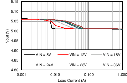
VOUT = 5 V FS = 500 kHz
Figure 9. VOUT Regulation
LM43601 C016_Reg_43601_5V2p2M.png
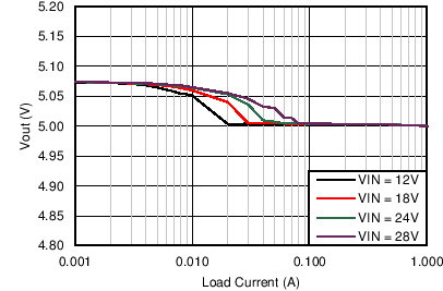
VOUT = 5 V FS = 2.2 MHz
Figure 11. VOUT Regulation
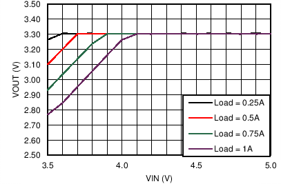
LM43601 C022_DO_43601_3p3V500k.png
VOUT = 3.3 V FS = 500 kHz
Figure 13. Dropout Curve
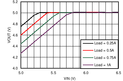
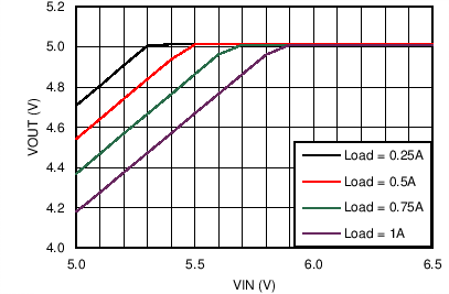
LM43601 C023_DO_43601_5V500k.png
VOUT = 5 V FS = 500 kHz
Figure 15. Dropout Curve
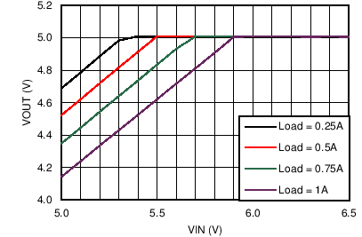
LM43601 C026_DO_43601_5V2p2M.png
VOUT = 5 V FS = 2.2 MHz
Figure 17. Dropout Curve
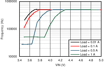
LM43601 43601_3V3_500kHz_Freq_Drop.png
VOUT = 3.3 V FS = 500 kHz
Figure 19. Switching Frequency vs VIN in Dropout Operation
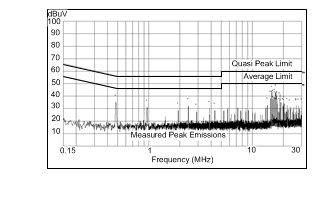
LM43601 LM43601_3p3_500k_Radiated.gif
VOUT = 3.3 V FS = 500 kHz IOUT = 1 A
Measured on the LM43601PWPEVM with default BOM. No input filter used.
Figure 21. Radiated EMI Curve
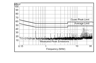
LM43601 LM43601_3p3_500k_Conducted.gif
VOUT = 3.3 V FS = 500 kHz IOUT = 1 A
Measured on the LM43601PWPEVM with default BOM. EVM Input filter: Lin = 1 µH Cd = 47 µF CIN4 = 68 µF
Figure 23. Conducted EMI Curve
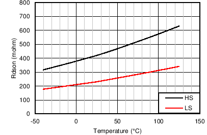
LM43601 Gen_Curve_On_Resistance.png
Figure 25. High-Side and Low-side On Resistance vs Junction Temperature
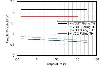
LM43601 Gen_Curve_EN_Threshold.png
Figure 27. Enable Threshold vs Junction Temperature
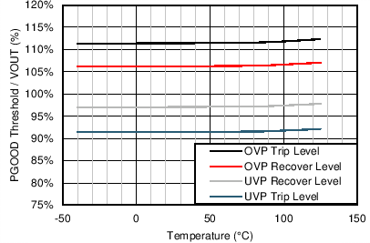
LM43601 Gen_Curve_PG_Threshold.png
Figure 29. PGOOD Threshold vs Junction Temperature
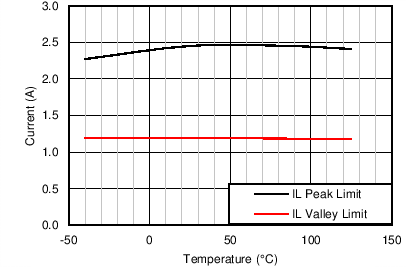
LM43601 Gen_Curve_46001Curr_Lim.png
VIN = 12 V VOUT = 3.3 V FS = 500 kHz
Figure 31. Peak and Valley Current Limits vs Junction Temperature
LM43601 C004_Eff_43601_5V200k.png
VOUT = 5 V FS = 200 kHz
Figure 2. Efficiency
LM43601 C005_Eff_43601_5V1M.png
VOUT = 5 V FS = 1 MHz
Figure 4. Efficiency
LM43601 C007_Eff_43601_12V500k.png
VOUT = 12 V FS = 500 kHz
Figure 6. Efficiency
LM43601 C014_Reg_43601_5V200k.png
VOUT = 5 V FS = 200 kHz
Figure 8. VOUT Regulation
LM43601 C015_Reg_43601_5V1M.png
VOUT = 5 V FS = 1 MHz
Figure 10. VOUT Regulation
LM43601 C017_Reg_43601_12V500k.png
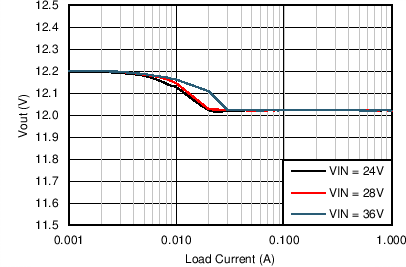
VOUT = 12 V FS = 500 kHz
Figure 12. VOUT Regulation
LM43601 C024_DO_43601_5V200k.png
VOUT = 5 V FS = 200 kHz
Figure 14. Dropout Curve
LM43601 C025_DO_43601_5V1M.png
VOUT = 5 V FS = 1 MHz
Figure 16. Dropout Curve
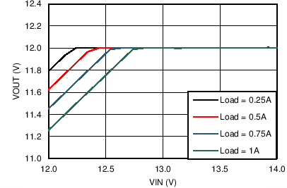
LM43601 C027_DO_43601_12V500k.png
VOUT = 12 V FS = 500 kHz
Figure 18. Dropout Curve
LM43601 43601_5V_1MHz_Freq_Drop.png
VOUT = 5 V FS = 1 MHz
Figure 20. Switching Frequency vs VIN in Dropout Operation
LM43601 LM43601_5_500k_Radiated.gif
VOUT = 5 V FS = 500 kHz IOUT = 1 A
Measured on the LM43601PWPEVM with L = 27 µH, COUT = 66 µF, CFF = 33 pF. No input filter used.
Figure 22. Radiated EMI Curve
LM43601 LM43601_5_500k_Conducted.gif
VOUT = 5 V FS = 500 kHz IOUT = 1 A
Measured on the LM43601PWPEVM with L = 18 µH, COUT = 66 µF, CFF = 33 pF. Input filter Lin = 1 µH Cd = 47 µF CIN4 = 68 µF
Figure 24. Conducted EMI Curve
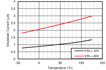
LM43601 Gen_Curve_Shdn_Current.png
Figure 26. Shutdown Current vs Junction Temperature
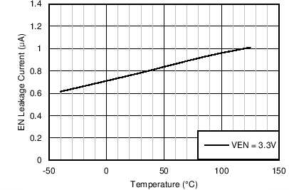
LM43601 Gen_Curve_EN_Leakage_Curr.png
Figure 28. Enable Leakage Current vs
Junction Temperature
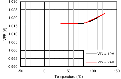
LM43601 Gen_Curve_FB_Voltage.png
Figure 30. Feedback Voltage vs Junction Temperature
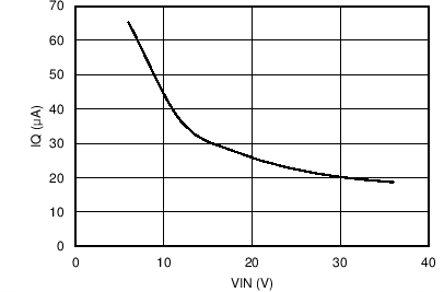
LM43601 Gen_Curve_43601Iq.png
VOUT = 3.3 V FS = 500 kHz IOUT = 0 A
Figure 32. Operating IQ vs VIN With BIAS Connected to VOUT