JAJSBZ3B June   2014  – March 2018 LM46000

PRODUCTION DATA.  

  1. 特長
  2. アプリケーション
  3. 概要
    1.     Device Images
      1.      概略回路図
      2.      放射エミッションのグラフ VOUT = 3.3V、VIN = 24V、FS= 500kHz、IOUT = 0.5A
  4. 改訂履歴
  5. Pin Configuration and Functions
    1.     Pin Functions
  6. Specifications
    1. 6.1 Absolute Maximum Ratings
    2. 6.2 ESD Ratings
    3. 6.3 Recommended Operating Conditions
    4. 6.4 Thermal Information
    5. 6.5 Electrical Characteristics
    6. 6.6 Timing Requirements
    7. 6.7 Switching Characteristics
    8. 6.8 Typical Characteristics
  7. Detailed Description
    1. 7.1 Overview
    2. 7.2 Functional Block Diagram
    3. 7.3 Feature Description
      1. 7.3.1  Fixed-Frequency, Peak-Current-Mode Controlled Step-Down Regulator
      2. 7.3.2  Light Load Operation
      3. 7.3.3  Adjustable Output Voltage
      4. 7.3.4  Enable (EN)
      5. 7.3.5  VCC, UVLO, and BIAS
      6. 7.3.6  Soft Start and Voltage Tracking (SS/TRK)
      7. 7.3.7  Switching Frequency (RT) and Synchronization (SYNC)
      8. 7.3.8  Minimum ON-Time, Minimum OFF-Time and Frequency Foldback at Dropout Conditions
      9. 7.3.9  Internal Compensation and CFF
      10. 7.3.10 Bootstrap Voltage (CBOOT)
      11. 7.3.11 Power Good (PGOOD)
      12. 7.3.12 Overcurrent and Short-Circuit Protection
      13. 7.3.13 Thermal Shutdown
    4. 7.4 Device Functional Modes
      1. 7.4.1 Shutdown Mode
      2. 7.4.2 Standby Mode
      3. 7.4.3 Active Mode
      4. 7.4.4 CCM Mode
      5. 7.4.5 Light Load Operation
      6. 7.4.6 Self-Bias Mode
  8. Applications and Implementation
    1. 8.1 Application Information
    2. 8.2 Typical Applications
      1. 8.2.1 Design Requirements
      2. 8.2.2 Detailed Design Procedure
        1. 8.2.2.1  Custom Design With WEBENCH® Tools
        2. 8.2.2.2  Output Voltage Setpoint
        3. 8.2.2.3  Switching Frequency
        4. 8.2.2.4  Input Capacitors
        5. 8.2.2.5  Inductor Selection
        6. 8.2.2.6  Output Capacitor Selection
        7. 8.2.2.7  Feed-Forward Capacitor
        8. 8.2.2.8  Bootstrap Capacitors
        9. 8.2.2.9  VCC Capacitor
        10. 8.2.2.10 BIAS Capacitors
        11. 8.2.2.11 Soft-Start Capacitors
        12. 8.2.2.12 Undervoltage Lockout Setpoint
        13. 8.2.2.13 PGOOD
      3. 8.2.3 Application Performance Curves
  9. Power Supply Recommendations
  10. 10Layout
    1. 10.1 Layout Guidelines
      1. 10.1.1 Compact Layout for EMI Reduction
      2. 10.1.2 Ground Plane and Thermal Considerations
      3. 10.1.3 Feedback Resistors
    2. 10.2 Layout Example
  11. 11デバイスおよびドキュメントのサポート
    1. 11.1 デバイス・サポート
      1. 11.1.1 WEBENCH®ツールによるカスタム設計
    2. 11.2 ドキュメントの更新通知を受け取る方法
    3. 11.3 コミュニティ・リソース
    4. 11.4 商標
    5. 11.5 静電気放電に関する注意事項
    6. 11.6 Glossary
  12. 12メカニカル、パッケージ、および注文情報

パッケージ・オプション

メカニカル・データ(パッケージ|ピン)
サーマルパッド・メカニカル・データ
発注情報

Application Performance Curves

See Table 2 for bill of materials for each VOUT and FS combination. Unless otherwise stated, application performance curves were taken at TA = 25°C.
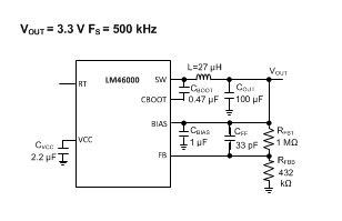
LM46000 Sch_BOM_3.3V500k.gif
VOUT = 3.3 V FS = 500 kHz VIN = 24 V
Figure 47. BOM for VOUT = 3.3 V FS = 500 kHz
LM46000 C012_Reg_46000_3p3V500k.png
VOUT = 3.3 V FS = 500 kHz
Figure 49. Output Voltage Regulation
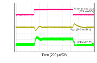
LM46000 24VIN_3p3VO_500k_50mATO500mA.gif
VOUT = 3.3 V FS = 500 kHz VIN = 24 V
Figure 51. Load Transient Between 0.05 A and 0.5 A
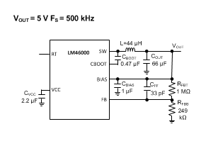
LM46000 Sch_BOM_5V500k.gif
VOUT = 5 V FS = 500 kHz VIN = 24 V
Figure 53. BOM for VOUT = 5 V, FS = 500 kHz
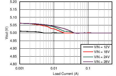
LM46000 C013_Reg_46000_5V500k.png
VOUT = 5 V FS = 500 kHz
Figure 55. Output Voltage Regulation
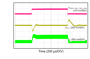
LM46000 24VIN_5VO_500k_50mATO500mA.gif
VOUT = 5 V FS = 500 kHz VIN = 24 V
Figure 57. Load Transient Between 0.05 A and 0.5 A
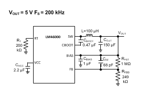
LM46000 Sch_BOM_5V200k.gif
VOUT = 5 V FS = 200 kHz VIN = 24 V
Figure 59. BOM for VOUT = 5 V, FS = 200 kHz
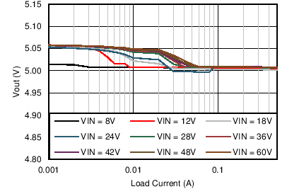
LM46000 C014_Reg_46000_5V200k.png
VOUT = 5 V FS = 200 kHz
Figure 61. Output Voltage Regulation
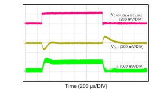
LM46000 24VIN_5VO_200k_50mATO500mA.gif
VOUT = 5 V FS = 200 kHz VIN = 24 V
Figure 63. Load Transient Between 0.05 A and 0.5A
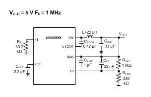
LM46000 Sch_BOM_5V1M.gif
VOUT = 5 V FS = 1 MHz VIN = 24 V
Figure 65. BOM for VOUT = 5 V, FS = 1 MHz
LM46000 C015_Reg_46000_5V1M.png
VOUT = 5 V FS = 1 MHz
Figure 67. Output Voltage Regulation
LM46000 24VIN_5VO_1M_50mATO500mA.gif
VOUT = 5 V FS = 1 MHz VIN = 24 V
Figure 69. Load Transient Between 0.05 A and 0.5 A
LM46000 Sch_BOM_12V500k.gif
VOUT = 12 V FS = 500 kHz VIN = 24 V
Figure 71. BOM for VOUT = 12 V, FS = 500 kHz
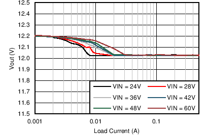
LM46000 C017_Reg_46000_12V500k.png
VOUT = 12 V FS = 500 kHz
Figure 73. Output Voltage Regulation
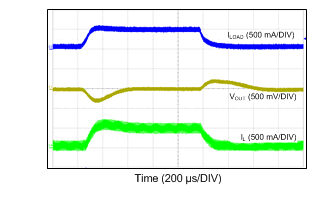
LM46000 24VIN_12VO_500k_50mATO500mA.gif
VOUT = 12 V FS = 500 kHz VIN = 24 V
Figure 75. Load Transient Between 0.05 A and 0.5 A
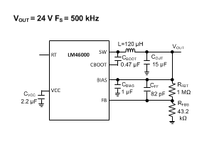
LM46000 Sch_BOM_24V500k.gif
VOUT = 24 V FS = 500 kHz VIN = 48 V
Figure 77. BOM for VOUT = 24 V, FS = 500 kHz
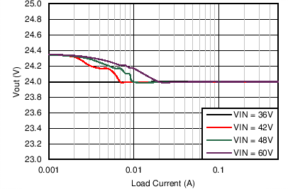
LM46000 C018_Reg_46000_24V500k.png
VOUT = 24 V FS = 500 kHz
Figure 79. Output Voltage Regulation
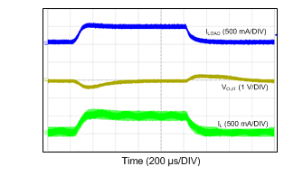
LM46000 48VIN_24VO_500k_50mATO500mA.gif
VOUT = 24 V FS = 500 kHz VIN = 48 V
Figure 81. Load Transient Between 0.05 A and 0.5 A
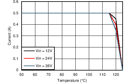
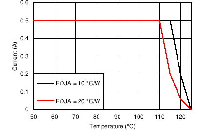
LM46000 3p3VO_500kThetaJA20CpW.png
VOUT = 3.3 V FS = 500 kHz RθJA = 20°C/W
Figure 83. Derating Curve With RθJA = 20°C/W
LM46000 5VO_200kThetaJA20CpW.png
VOUT = 5 V FS = 200 kHz RθJA = 20°C/W
Figure 85. Derating Curve With RθJA = 20°C/W
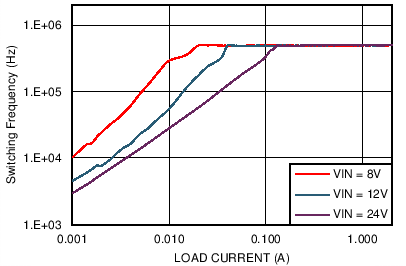
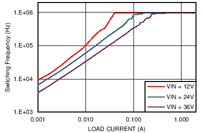
LM46000 3p3V_500k_Fsw_PFM.png
VOUT = 3.3 V FS = 500 kHz
Figure 87. Switching Frequency vs IOUT in PFM Operation
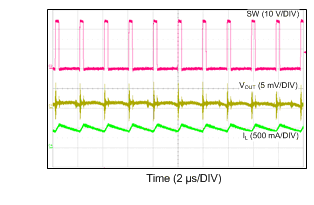
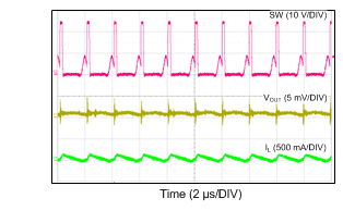
LM46000 24VIN_3V3_500k_500mA_CCM.gif
VOUT = 3.3 V FS = 500 kHz IOUT = 0.5A
Figure 89. Switching Waveform in CCM Operation
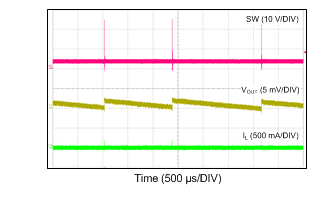
LM46000 24VIN_3V3_500k_0mA_PFM.gif
VOUT = 3.3 V FS = 500 kHz IOUT = 0 mA
Figure 91. Switching Waveform in PFM Operation
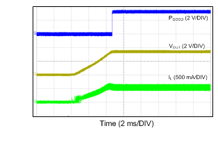
LM46000 24VIN_3p3VO_500k_250mA.gif
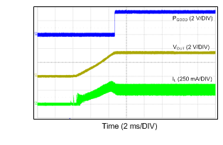
VIN = 24 V VOUT = 3.3 V RLOAD = 13.2 Ω
Figure 93. Start-up Into Half Load With Internal Soft-Start Rate
LM46000 24VIN_3p3VO_500k_PREBIAS_1V.gif
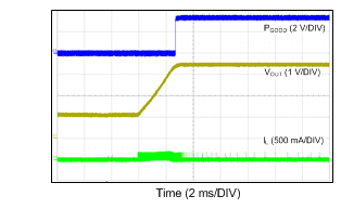
VIN = 24 V VOUT = 3.3 V RLOAD = Open
Figure 95. Start-up Into 1.0 V Pre-biased Voltage
LM46000 12TO48V_3V3_500k_500mA_1V1us.gif
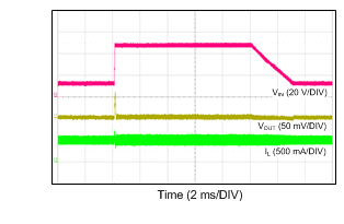
VOUT = 3.3 V FS = 500 kHz IOUT = 0.5A
Figure 97. Line Transient: VIN Transitions Between 12 V and 48 V
LM46000 24VIN_3p3VO_500k_500mA_SHORT_RECOVERY.gif
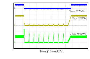
VOUT = 3.3 V FS = 500 kHz VIN = 24 V
Figure 99. Short-Circuit Protection and Recover
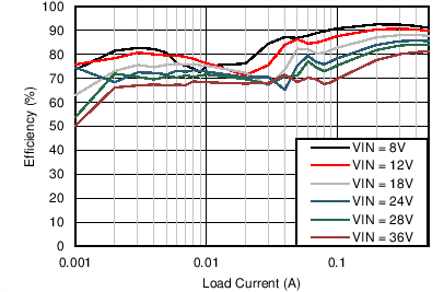
LM46000 C002_Eff_46000_3p3V500k.png
VOUT = 3.3 V FS = 500 kHz
Figure 48. Efficiency
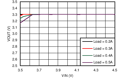
LM46000 C022_DO_46000_3p3V500k.png
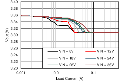
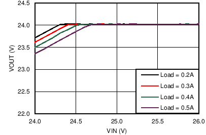
VOUT = 3.3 V FS = 500 kHz
Figure 50. Dropout Curve
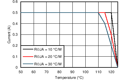
LM46000 24V_3p3VO_500kThetaJA.png
VOUT = 3.3 V FS = 500 kHz VIN = 24 V
Figure 52. Derating Curve
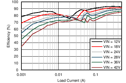
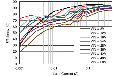
LM46000 C003_Eff_46000_5V500k.png
VOUT = 5 V FS = 500 kHz
Figure 54. Efficiency
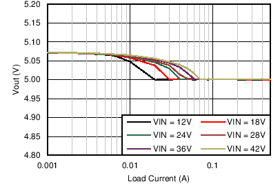
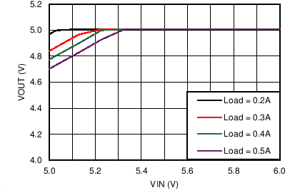
LM46000 C023_DO_46000_5V500k.png
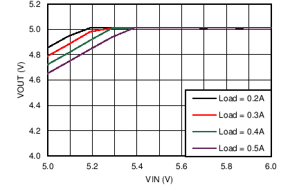
VOUT = 5 V FS = 500 kHz
Figure 56. Dropout Curve
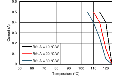
LM46000 24V_5VO_500kThetaJA.png
VOUT = 5 V FS = 500 kHz VIN = 24 V
Figure 58. Derating Curve
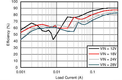
LM46000 C004_Eff_46000_5V200k.png
VOUT = 5 V FS = 200 kHz
Figure 60. Efficiency
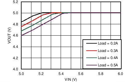
LM46000 C024_DO_46000_5V200k.png
VOUT = 5 V FS = 200 kHz
Figure 62. Dropout Curve
LM46000 24V_5VO_200kThetaJA.png
VOUT = 5 V FS = 200 kHz VIN = 24 V
Figure 64. Derating Curve
LM46000 C005_Eff_46000_5V1M.png
VOUT = 5 V FS = 1 MHz VIN = 24 V
Figure 66. Efficiency
LM46000 C025_DO_46000_5V1M.png
VOUT = 5 V FS = 1 MHz
Figure 68. Dropout Curve
LM46000 24V_5VO_1000kThetaJA.png
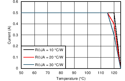
VOUT = 5 V FS = 1 MHz VIN = 24 V
Figure 70. Derating Curve
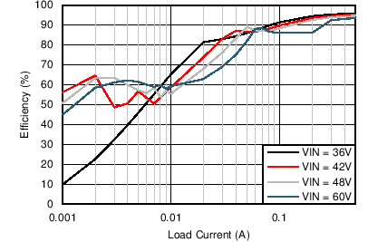
LM46000 C007_Eff_46000_12V500k.png
VOUT = 12 V FS = 500 kHz
Figure 72. Efficiency
LM46000 C027_DO_46000_12V500k.png
VOUT = 12 V FS = 500 kHz
Figure 74. Dropout Curve
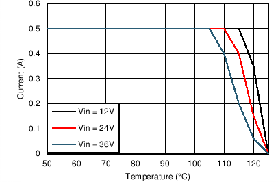
LM46000 24V_12VO_500kThetaJA.png
VOUT = 12 V FS = 500 kHz VIN = 24 V
Figure 76. Derating Curve
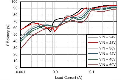
LM46000 C008_Eff_46000_24V500k.png
VOUT = 24 V FS = 500 kHz
Figure 78. Efficiency
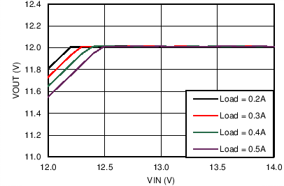
LM46000 C028_DO_46000_24V500k.png
VOUT = 24 V FS = 500 kHz
Figure 80. Dropout Curve
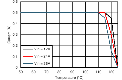
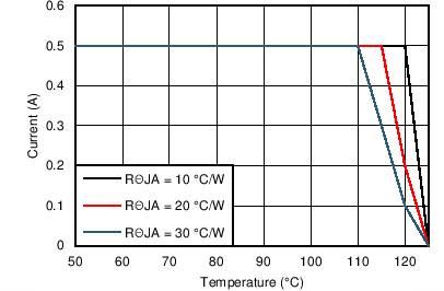
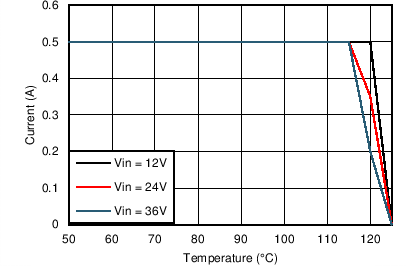
LM46000 48V_24VO_500kThetaJA.png
VOUT = 24 V FS = 500 kHz VIN = 48 V
Figure 82. Derating Curve
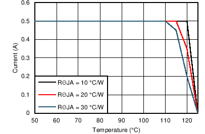
LM46000 5VO_500kThetaJA20CpW.png
VOUT = 5 V FS = 500 kHz RθJA = 20°C/W
Figure 84. Derating Curve With RθJA = 20°C/W
LM46000 5VO_1000kThetaJA20CpW.png
VOUT = 5 V FS = 1 MHz RθJA = 20°C/W
Figure 86. Derating Curve With RθJA = 20°C/W
LM46000 5V_1M_Fsw_PFM.png
VOUT = 5 V FS = 1 MHz
Figure 88. Switching Frequency vs IOUT in PFM Operation
LM46000 24VIN_3V3_500k_40mA_DCM.gif
VOUT = 3.3 V FS = 500 kHz IOUT = 40 mA
Figure 90. Switching Waveform in DCM Operation
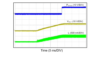
LM46000 24VIN_3p3VO_500k_500mA.gif
VIN = 24 V VOUT = 3.3 V RLOAD = 6.6 Ω
Figure 92. Start-up Into Full Load With Internal Soft-Start Rate
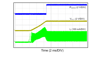
LM46000 24VIN_3p3VO_500k_100mA.gif
VIN = 24 V VOUT = 3.3 V RLOAD = 33 Ω
Figure 94. Start-up Into 100 mA With Internal Soft-Start Rate
LM46000 24VIN_12VO_500k_500mA_33nFCss.gif
VIN = 24 V VOUT = 12 V RLOAD = 24 Ω
Figure 96. Start-up With External Capacitor CSS = 33 nF
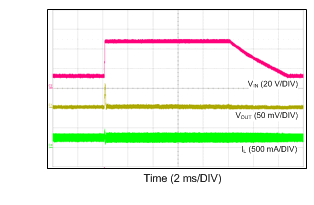
LM46000 12TO48V_3V3_500k_250mA_1V1us.gif
VOUT = 3.3 V FS = 500 kHz IOUT = 0.25 A
Figure 98. Line Transient: VIN Transitions Between 12 V and 48 V