JAJSBJ6H March   2009  – October 2018 LM5008A

PRODUCTION DATA.  

  1. 特長
  2. アプリケーション
  3. 概要
    1.     Device Images
      1.      代表的なアプリケーション: 基本的な降圧レギュレータ
  4. 改訂履歴
  5. Pin Configuration and Functions
    1.     Pin Functions
  6. Specifications
    1. 6.1 Absolute Maximum Ratings
    2. 6.2 ESD Ratings
    3. 6.3 Recommended Operating Conditions
    4. 6.4 Thermal Information
    5. 6.5 Electrical Characteristics
    6. 6.6 Switching Characteristics
    7. 6.7 Typical Characteristics
  7. Detailed Description
    1. 7.1 Overview
    2. 7.2 Functional Block Diagram
    3. 7.3 Feature Description
      1. 7.3.1 Control Circuit Overview
      2. 7.3.2 Start-Up Regulator (VCC)
      3. 7.3.3 Regulation Comparator
      4. 7.3.4 Overvoltage Comparator
      5. 7.3.5 On-Time Generator and Shutdown
      6. 7.3.6 Current Limit
      7. 7.3.7 N-Channel Buck Switch and Driver
      8. 7.3.8 Thermal Protection
    4. 7.4 Device Functional Modes
      1. 7.4.1 Shutdown Mode
      2. 7.4.2 Active Mode
  8. Application and Implementation
    1. 8.1 Application Information
    2. 8.2 Typical Application
      1. 8.2.1 Design Requirements
      2. 8.2.2 Detailed Design Procedure
        1. 8.2.2.1 Custom Design With WEBENCH® Tools
        2. 8.2.2.2 Selection Of External Components
        3. 8.2.2.3 Low-Output Ripple Configurations
      3. 8.2.3 Application Curves
  9. Power Supply Recommendations
  10. 10Layout
    1. 10.1 Layout Guidelines
    2. 10.2 Layout Example
  11. 11デバイスおよびドキュメントのサポート
    1. 11.1 デバイス・サポート
      1. 11.1.1 デベロッパー・ネットワークの製品に関する免責事項
      2. 11.1.2 WEBENCH®ツールによるカスタム設計
      3. 11.1.3 開発サポート
    2. 11.2 ドキュメントのサポート
      1. 11.2.1 関連資料
        1. 11.2.1.1 PCBレイアウトについてのリソース
        2. 11.2.1.2 熱設計についてのリソース
    3. 11.3 ドキュメントの更新通知を受け取る方法
    4. 11.4 コミュニティ・リソース
    5. 11.5 商標
    6. 11.6 静電気放電に関する注意事項
    7. 11.7 Glossary
  12. 12メカニカル、パッケージ、および注文情報

パッケージ・オプション

メカニカル・データ(パッケージ|ピン)
サーマルパッド・メカニカル・データ
発注情報

On-Time Generator and Shutdown

The on-time for the LM5008A is determined by the RT resistor and is inversely proportional to the input voltage (VIN), resulting in a nearly constant frequency as Vin is varied over its range. The on-time equation for the LM5008A is Equation 4.

Equation 4. TON = 1.385 × 10⁻¹⁰ × RT / VIN

RT must be selected for a minimum on-time (at maximum VIN) greater than 400 ns, for proper current limit operation. This requirement limits the maximum frequency for each application, depending on VIN and VOUT.

The LM5008A can be remotely disabled by taking the RT/SD pin to ground. See Figure 9. The voltage at the RT/SD pin is between 1.5 V and 3 V, depending on VIN and the value of the RT resistor.
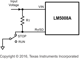
LM5008A 30074915.gifFigure 9. Shutdown Implementation