JAJSF96C April 2018 – October 2021 LM5036
PRODUCTION DATA
- 1 特長
- 2 アプリケーション
- 3 概要
- 4 Revision History
- 5 Pin Configuration and Functions
- 6 Specifications
-
7 Detailed Description
- 7.1 Overview
- 7.2 Functional Block Diagram
- 7.3
Feature Description
- 7.3.1 High-Voltage Start-Up Regulator
- 7.3.2 Undervoltage Lockout (UVLO)
- 7.3.3 Reference Regulator
- 7.3.4 Oscillator, Synchronized Input
- 7.3.5 Voltage-Mode Control
- 7.3.6 Primary-Side Gate Driver Outputs (LSG and HSG)
- 7.3.7 Half-Bridge PWM Scheme
- 7.3.8 Maximum Duty Cycle Operation
- 7.3.9 Pre-Biased Start-Up Process
- 7.3.10 Zero Duty Cycle Operation
- 7.3.11 Enhanced Cycle-by-Cycle Current Limiting with Pulse Matching
- 7.3.12 Reverse Current Protection
- 7.3.13 CBC Threshold Accuracy
- 7.3.14 Hiccup Mode Protection
- 7.3.15 Hiccup Mode Blanking
- 7.3.16 Over-Temperature Protection (OTP)
- 7.3.17 Over-Voltage / Latch (ON_OFF Pin)
- 7.3.18 Auxiliary Constant On-Time Control
- 7.3.19 Auxiliary On-Time Generator
- 7.3.20 Auxiliary Supply Current Limiting
- 7.3.21 Auxiliary Primary Output Capacitor Ripple
- 7.3.22 Auxiliary Ripple Configuration and Control
- 7.3.23 Asynchronous Mode Operation of Auxiliary Supply
- 7.4 Device Functional Modes
-
8 Application and Implementation
- 8.1 Application Information
- 8.2
Typical Application
- 8.2.1 Design Requirements
- 8.2.2
Detailed Design Procedure
- 8.2.2.1 Custom Design With WEBENCH® Tools
- 8.2.2.2 Input Transient Protection
- 8.2.2.3 Level-Shift Detection Circuit
- 8.2.2.4 Applications with VIN > 100-V
- 8.2.2.5 Applications without Pre-Biased Start-Up Requirement
- 8.2.2.6 UVLO Voltage Divider Selection
- 8.2.2.7 Over Voltage, Latch (ON_OFF Pin) Voltage Divider Selection
- 8.2.2.8 SS Capacitor
- 8.2.2.9 SSSR Capacitor
- 8.2.2.10 Half-Bridge Power Stage Design
- 8.2.2.11 Current Limit
- 8.2.2.12 Auxiliary Transformer
- 8.2.2.13 Auxiliary Feedback Resistors
- 8.2.2.14 RON Resistor
- 8.2.2.15 VIN Pin Capacitor
- 8.2.2.16 Auxiliary Primary Output Capacitor
- 8.2.2.17 Auxiliary Secondary Output Capacitor
- 8.2.2.18 Auxiliary Feedback Ripple Circuit
- 8.2.2.19 Auxiliary Secondary Diode
- 8.2.2.20 VCC Diode
- 8.2.2.21 Opto-Coupler Interface
- 8.2.2.22 Full-Bridge Converter Applications
- 8.2.3 Application Curves
- 9 Power Supply Recommendations
- 10Layout
- 11Device and Documentation Support
- 12Mechanical, Packaging, and Orderable Information
7.3.5 Voltage-Mode Control
The LM5036 device employs voltage-mode control with input voltage feed-forward for the main half-bridge converter. A simplified block diagram of the voltage-mode feedback control loop is shown in Figure 7-2.
 Figure 7-2 Voltage-Mode Feedback Control Loop for Half-Bridge Converter
The output voltage (VO) is sensed and compared against a reference voltage (VREFSec) on the secondary side which produces an error voltage which is then processed by the error amplifier. The compensated error signal is transmitted across the isolation boundary through an opto-coupler and then gets injected into the COMP pin in the form of a control current. The COMP pin current is internally mirrored by a matching pair of NPN transistors which sink current through a 5-kΩ resistor connected to the 5-V internal reference. The resulting control voltage VCOMP is compared with the soft-start capacitor voltage (SS) and the smaller of the two passes through an offset VSS-OS (1-V typical), followed by a 2:1 resistor divider before being applied to the PWM comparator to determine the duty cycle of the half-bridge converter. The PWM comparator polarity is configured such that with no current flowing into the COMP pin, the controller produces maximum duty cycle for the primary FETs.
An opto-coupler detector can be connected between the REF pin and the COMP pin. Because the COMP pin is controlled by a current input, the voltage across the opto-coupler detector is nearly constant. The bandwidth limiting phase delay which is normally introduced by the significant capacitance of the opto-coupler is thereby greatly reduced. Higher loop bandwidths can be realized because the bandwidth limiting pole associated with the opto-coupler is now at a much higher frequency.
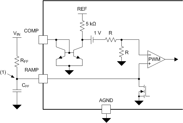
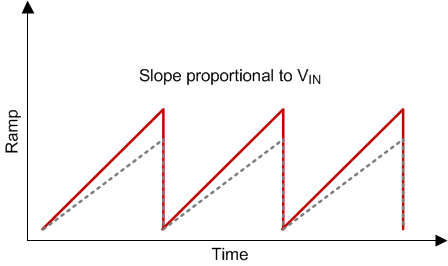
The voltage at the RAMP pin provides the modulation ramp for the PWM comparator. The PWM comparator compares the modulation ramp signal at the RAMP pin to the COMP voltage to control the duty cycle. The modulation ramp signal can be implemented as a ramp proportional to the input voltage, known as feed-forward voltage mode control, as shown in Figure 7-3. The RAMP pin is reset by an internal MOSFET when RAMP voltage passes COMP voltage, current limit event, or at the conclusion of each PWM cycle, whichever comes earlier.

 Figure 7-4 Modulation Ramp
Slope
Figure 7-4 Modulation Ramp
SlopeAn external resistor (RFF) and capacitor (CFF) connected to VIN, AGND, and the RAMP pins are required to create a saw-tooth modulation ramp signal. The slope of the signal at RAMP will vary in proportion to the input voltage. The varying slope provides line feed-forward information necessary to improve line transient response with voltage-mode control. With a constant control signal, the on-time (tON) varies inversely with the input voltage (VIN) to stabilize the volt-second product of the transformer. Using a line feed-forward ramp for PWM control requires very little change in the voltage regulation loop to compensate for changes in input voltage, as compared to a ramp with fixed slope. In addition, voltage-mode control is less susceptible to noise. Therefore, it is a good choice for wide input range power converter applications. However, voltage-mode control requires a Type-III compensation network due to the complex-conjugate poles of the L-C output filter.
Assistance with half-bridge voltage control loop design may be obtained using the Power Stage Designer™ tool.
The recommended capacitor value range for CFF is from 100-pF to 1800-pF. Figure 7-3, shows that the CFF value must be small enough to be discharged within the clock pulse-width (tCLK). The value of RFF required can be calculated from Equation 2

For example, assuming a VRAMP voltage of 1.5-V (a good compromise of signal range and noise immunity), VIN(min) of 36-V, oscillator frequency of 400-kHz and CFF = 560-pF results in RFF = 105-kΩ.